


Everbright's Comprehensive Product Portfolio Empowering Global Markets: Cutting-Edge Technology and Mature Solutions Shine at the Laser World of Photonincs 2025!
06/27
2025
From June 24 to 27, the world's leading laser, optics, and optoelectronics industry event LASER World of Photonics was held in Munich, Germany. This exhibition is held every two years and has become an important platform to showcase cutting-edge optoelectronic technologies and promote industry exchange and cooperation. It attracts top companies, research institutions, and industry experts from around the world every year. Changguang Huaxin showcased its full range of products. Hall A2, Booth 311 Booth!
Full product matrix Empowering diverse applications
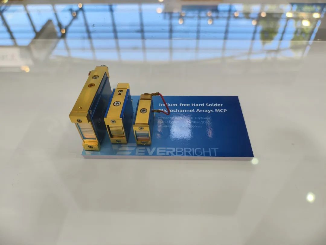
Changguang Huaxin made a grand appearance with its full product matrix, covering three core areas: high-power semiconductor laser chips, high-speed optical communication chips, and LiDAR/3D sensing chips, along with supporting devices, pump source modules, and array module complete solutions. Fully empowering diverse application scenarios such as industrial manufacturing, communication transmission, intelligent sensing, medical aesthetics, and new displays, fully demonstrating the technical strength and mass production advantages of the IDM full industry chain platform.
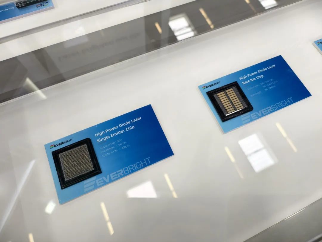
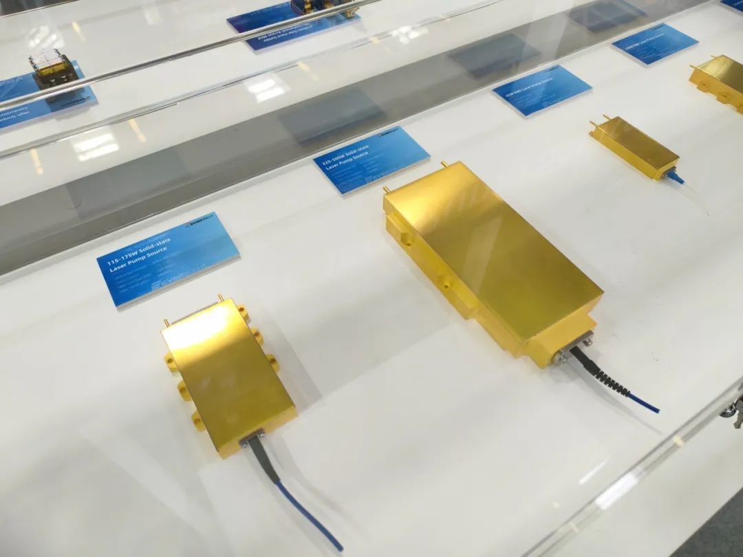
Industrial Manufacturing:
250W 9XXnm bar chip
500W 888nm solid-state laser pump source
300W 976±0.5nm fiber laser pump source
Communication Transmission:
200G PAM4 EML chip
70mW CWDM4 CW chip
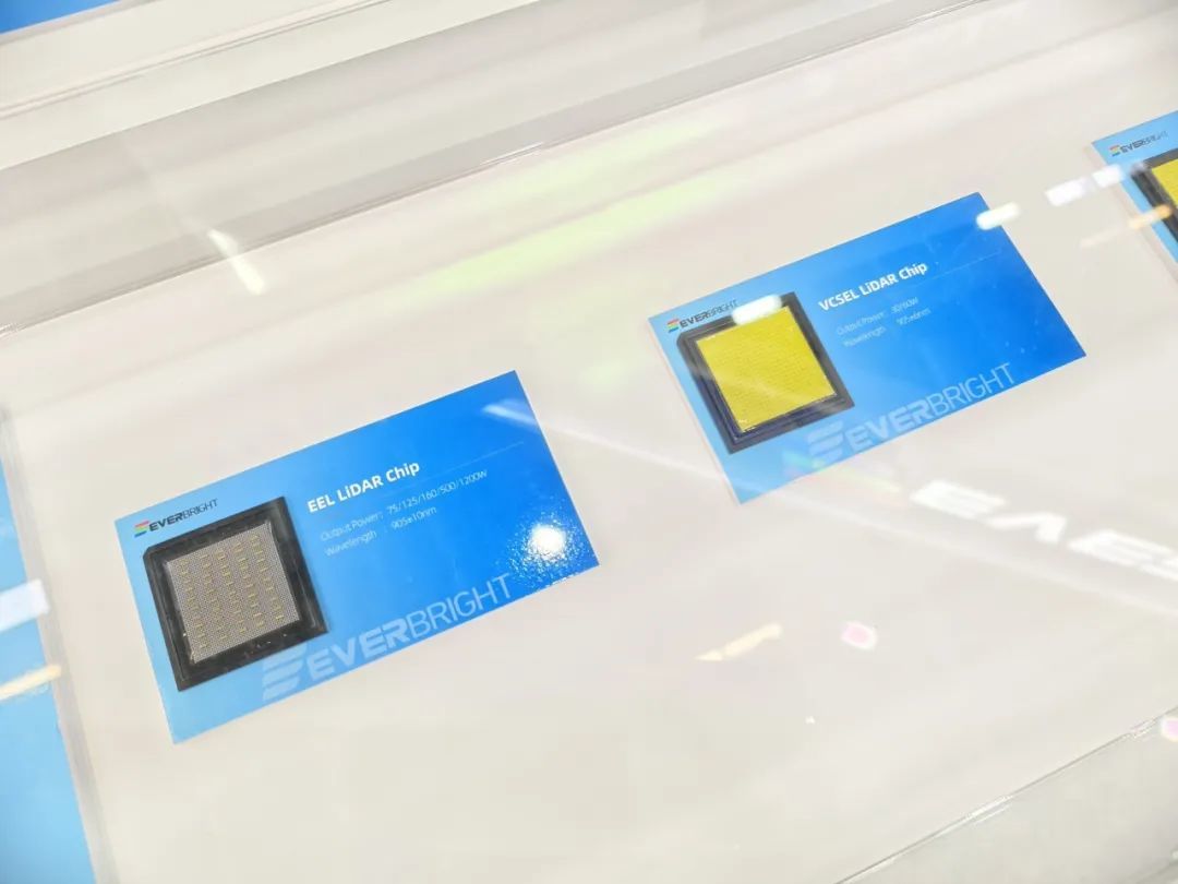
Radar Sensing:
4.6μm QCL quantum cascade laser chip
905nm 300W VCSEL LiDAR chip
Medical Aesthetics:
1726nm fiber-coupled module (acne treatment)
792nm fiber-coupled module (laser lithotripsy, skin rejuvenation)
1470nm fiber-coupled module (varicose vein treatment)
Laser Nuclear Fusion:
88Xnm 600W bar chip
940nm 700W (QCW) bar chip
940nm 56000W (QCW) V80 array
Hardcore technology + mature solutions
Dual engines driving overseas market expansion
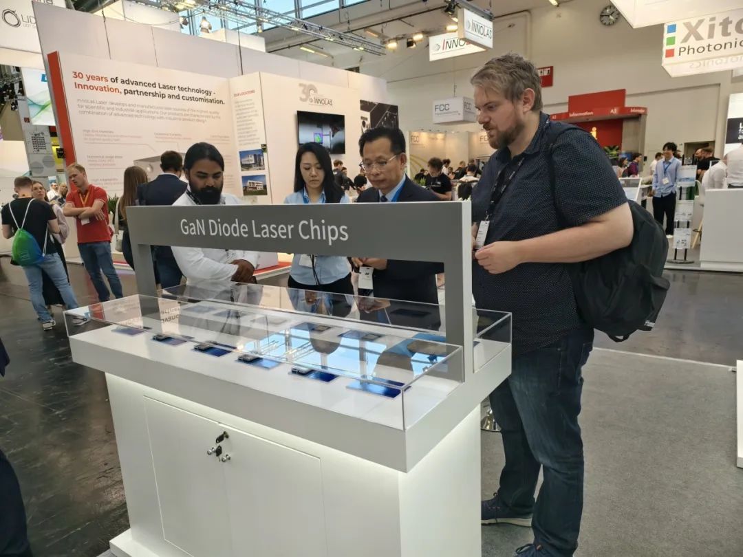
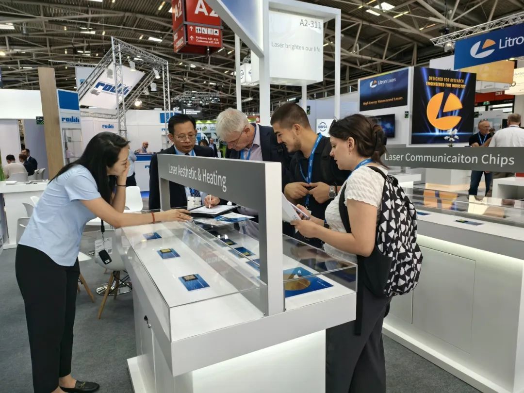
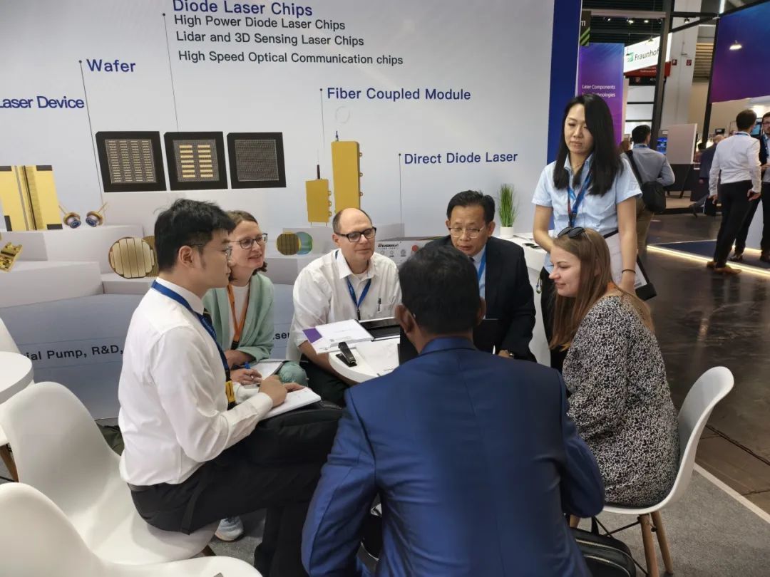
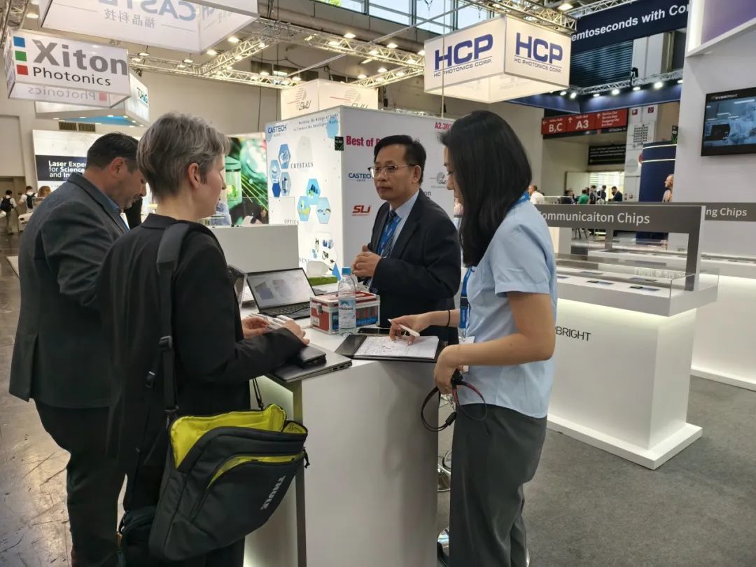
Changguang Huaxin's hardcore technology and mature industry solutions attracted many professional visitors for consultation and exchange, with the booth bustling with popularity!
3 major technology platforms, 5 major material systems, 2 major technology routes, numerous application scenarios... A2.311 awaits your discovery.
Changguang Huaxin has built a vertical production line for semiconductor laser chips covering 2-inch, 3-inch, and 6-inch wafers, featuring both edge-emitting (EEL) and vertical-cavity surface-emitting (VCSEL) dual technology routes, and mastering core processes for five major material systems: gallium arsenide (GaAs), indium phosphide (InP), gallium nitride (GaN), silicon carbide (SiC), and silicon photonics (SiPh). Relying on an independently controllable IDM full-process platform, the company can quickly respond to market demands and efficiently iterate cutting-edge products. Through a three-dimensional industrial layout of "multi-size wafers + dual technology architecture + multi-material platform," it continuously provides innovative solutions for fields such as photonic manufacturing, optical communication, optical sensing, photonic medical treatment, and photonic displays, leading industry technology upgrades!
The exhibition is still in full swing, and we are waiting for you at booth A2.311!
Recommended Reading

Address: No.56,Lijiang Road,SND,Suzhou,Jiangsu Province,P.R.China
Mailbox:sales@everbrightphotonics.com
Website:www.everbrightphotonics.com
Phone:+86 0512-66896988
Fax:+86 0512-66806323
Message Board