


The "Super Power" of Industrial Intelligent Manufacturing | An Article Explaining Changguang Huaxin's Three Major System Solutions
01/09
2024
Laser is a "super tool" in high-end intelligent manufacturing. Among them, laser welding is widely used in fields such as mechanical manufacturing, automotive industry, and microelectronics due to its multiple advantages including high quality, high precision, low deformation, and high efficiency.
Driven by customer demand, Changguang Huaxin has launched targeted solutions for fields such as laser soldering, furniture edge banding, and Mini/Micro LED laser mass welding.

Changguang Huaxin 9XXnm hundred-watt level semiconductor laser
Laser wavelength band has good thermal effect and uniform beam energy
Changguang Huaxin direct Semiconductor laser The output beam wavelength is 915nm and 976nm, producing good spot uniformity and excellent beam quality, enabling uniform heating of solder pads.
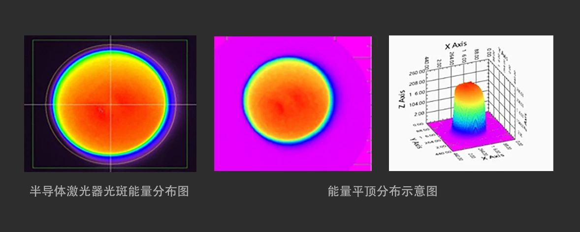
Non-contact processing, adjustable spot size
Adapted for complex structure soldering
Throughout the processing, there is no contact with the workpiece, so it will not produce Contact stress Using laser beam instead of soldering iron to heat the solder is more suitable for complex structure soldering.
Imported high-precision temperature probe
Accurate temperature detection, precise control of soldering temperature
Using high-precision imported infrared temperature probe combined with self-developed temperature control system to accurately capture beam temperature, then feedback to adjust laser output power, achieving precise control of the soldering process.
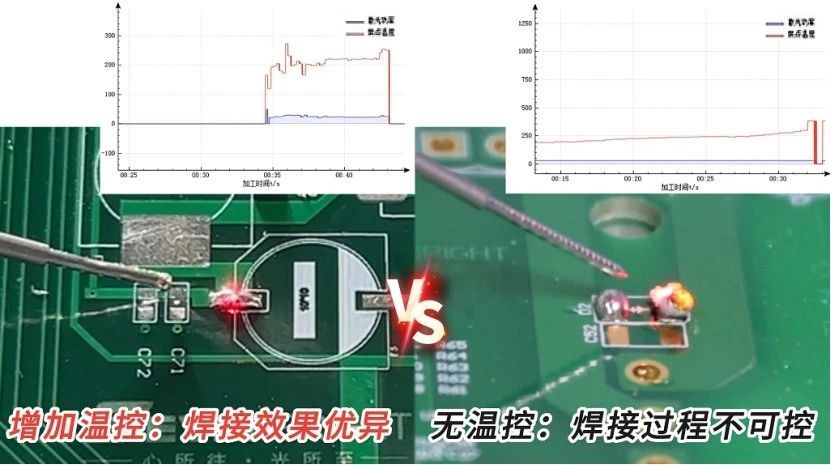
Changguang Huaxin solder joint temperature control system paired with hundred-watt level direct semiconductor laser helps the development of the soldering industry.
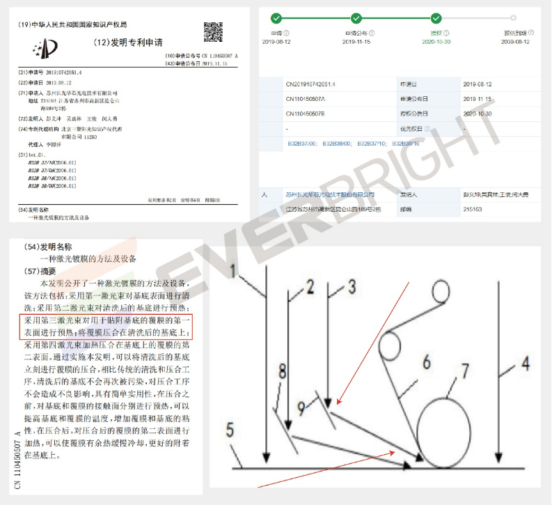
"A method and device for laser coating" invention patent
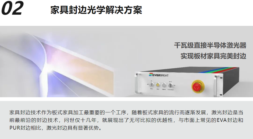
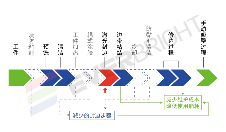
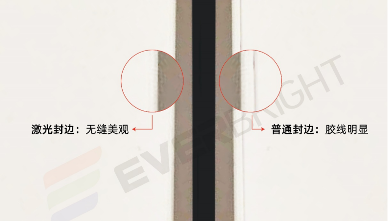
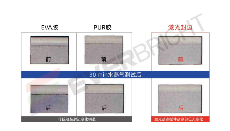
This patented technology mainly describes a method using a direct semiconductor laser as a heating light source to heat the film layer and press the film layer with the coating surface. Verified in the market, the shaped spot morphology of the direct semiconductor laser is suitable for this edge banding application. The energy distribution emitted by the direct semiconductor laser is uniform, and the actual welding effect is superior to traditional lasers.
The kilowatt-level direct semiconductor laser adopts a compact design, occupying a small footprint, generating less waste heat, efficiently converting electrical energy, greatly extending the laser's service life, and is safe and intelligent with easy operation. It is equipped with a variable focus optical lens that can present various rectangular spots according to customer needs for edge band heating, providing customers with perfect solutions.
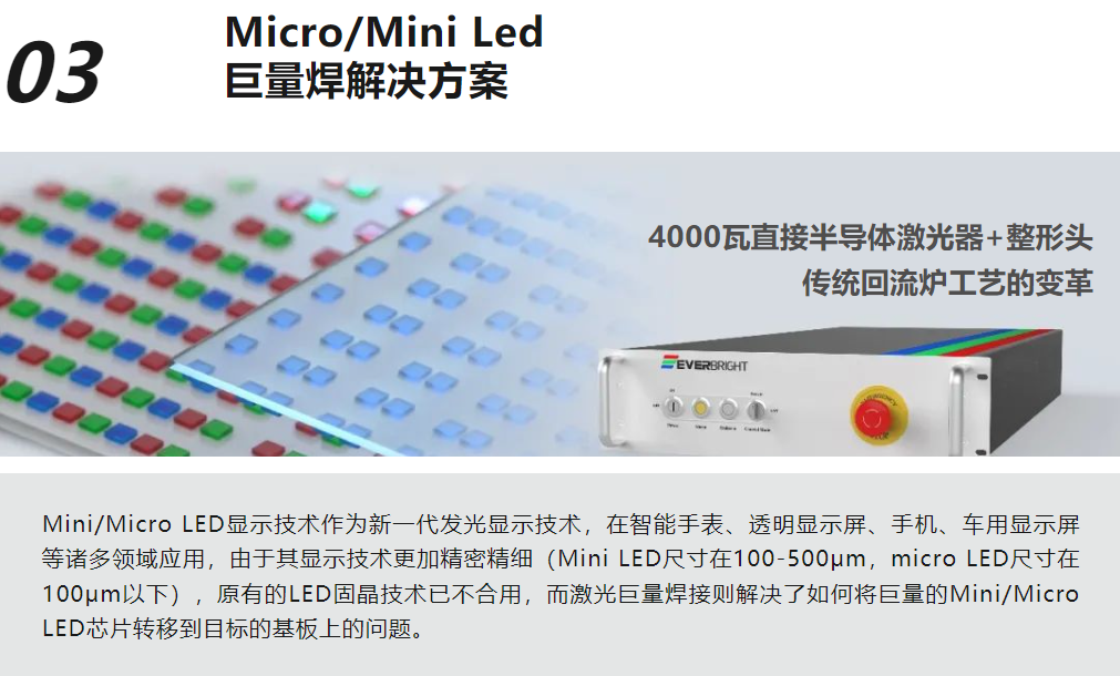
Nowadays, chip size and quality are extremely delicate. After chip transfer, using traditional reflow ovens is very difficult because slight vibrations may cause chip displacement. Also, due to thermal stress, slight warping can cause chip displacement. Changguang Huaxin's Micro/Mini LED mass welding solution with a 4000-watt direct semiconductor laser paired with a shaping head perfectly meets customer needs. It not only ensures good weld quality without warping but also has very high efficiency and energy saving, replacing traditional reflow oven processes.
Laser batch welding uses micro-beam shaping technology to transform the laser beam into a large-area homogeneous beam, then uses this beam to heat the mini or micro LED board area, enabling one-time welding of the LED chip irradiation area to achieve large-scale welding.
Recommended Reading

Address: No.56,Lijiang Road,SND,Suzhou,Jiangsu Province,P.R.China
Mailbox:sales@everbrightphotonics.com
Website:www.everbrightphotonics.com
Phone:+86 0512-66896988
Fax:+86 0512-66806323
Message Board