


Major Breakthrough | Changguang Huaxin High-Power Semiconductor Single-Tube Chip Continuous Output Power Exceeds 132W
03/25
2024
Changguang Huaxin first announced a single-chip with over 100W in February, and this research achievement was officially published in the internationally renowned SCI journal "photonics". The double-junction single-chip laser has a continuous wave power exceeding 132W at room temperature (about twice the maximum power of single-chip lasers reported in the literature), representing the highest power level reported for single-chip lasers to date, continuously leading the technological development in the high-power chip industry. The article is titled "Double-Junction Cascaded GaAs-Based Broad-Area Diode Lasers with 132W Continuous Wave Output Power."
Journal number: Photonics 2024, 11(3), 258;
Original link: https://www.mdpi.com/2304-6732/11/3/258
1. Introduction
High-power broad-area semiconductor lasers (BALs) have become the main pump sources , widely used in industrial fields, thanks to their high power conversion efficiency, high reliability, and low cost [1-17]. The rapid development in fiber lasers and solid-state lasers has led to increasing demand for semiconductor lasers with higher output power and conversion efficiency.
In the past 20 years, significant progress has been made in power and efficiency improvements [7-13]. In 2008, Petrescu-Prahova et al. demonstrated BALs with a 100-micron injection width, achieving a dual-end output power of 25.3 W at room temperature [14]. Subsequently, in 2017, V. Gapontsev et al. reported BALs with output power exceeding 30W [15]. In 2022, Yuxian Liu et al. further increased the output power, reaching 48 W for a single chip [16]. In 2023, we demonstrated BALs operating at room temperature with a 230-micron injection width, providing 51 W output power [17]. Further major progress must be based on a more detailed analysis of power and efficiency limitations.
As the drive current increases, all lasers experience power saturation and a decrease in quantum efficiency. An important factor is the Joule heating which causes the temperature of the active region to rise, broadening the gain and reducing the peak gain, thereby limiting further increases in output power. To address this issue, based on our tunnel junction technology [18], double-junction lasers were developed, achieving a significant improvement. Compared with conventional devices, double-junction devices can achieve higher output power at lower current and less Joule heating. Previously, multi-junction technology had made great breakthroughs and was widely used in short-pulse vertical-cavity surface-emitting lasers (VCSELs) and LiDAR systems [19-23]. However, the application of multi-junction technology in continuous-wave lasers is limited by issues such as thermal management, lateral mode control, multi-junction failure, and fiber coupling, resulting in relatively few reports on multi-junction cascaded technology in continuous-wave lasers.
This paper provides a comprehensive analysis of double-junction GaAs-based broad-area semiconductor lasers (double-junction BALs), highlighting their ability to achieve ultra-high continuous laser output power at room temperature. We conducted electro-optical simulations and design studies of double-junction BALs. Simulation results show that at room temperature, double-junction BALs reduce Joule heating generation at the same output power. The double-junction structure does not significantly affect heat transfer within the device. Meanwhile, based on single-junction devices with low internal loss and thermal stability, high-power BALs with different junction numbers were fabricated and their output characteristics precisely compared. Experimental results show that double-junction BALs achieve a maximum output power of 132.5 W under room temperature and DC drive, which is the highest power reported so far. In addition, the corresponding power conversion efficiency remains at 60%, with peak efficiency close to 70%. Compared with single-junction BALs, at the same output power, double-junction BALs reduce the optical power density at the output cavity facet by 50%, significantly improving device reliability.
2. Simulation and Design
In Figure 1a, we show the epitaxial structure of the double-junction BALs. The double-junction BALs are formed by cascading two single-junction BALs with the same active region, waveguide layer, and confinement layers through a GaAs tunnel junction. The epitaxial structure of the single-junction BAL includes a single InGaAs/AlGaAs quantum well, AlGaAs waveguide layer, n-type AlGaAs confinement layer, and p-type AlGaAs confinement layer. To clearly show the structural details, Figure 1b depicts the refractive index distribution of the single-junction BAL in the epitaxial direction and the fundamental mode distribution. The device injection width and cavity length are 500 μm and 5.6 mm, respectively. The front and rear cavity reflectivities are 1.5% and 99%, respectively. We used Crosslight software to establish the simulation model, adopting a one-dimensional carrier and optical model, without considering thermal effects in the simulation. Meanwhile, experimental data of single-junction BALs at room temperature were used to calibrate the simulation model. We calculated the L-I-V characteristics, output power, and conversion efficiency of single-junction and double-junction laser structures, and simulated the device temperature characteristics using the finite element method. It should be noted that the internal quantum efficiency was assumed constant in the simulation. The simulation results are shown in Figure 2. Figure 2a shows that if the injection width remains unchanged, the output power increases with the number of junctions. Assuming sufficient heat dissipation capability, the injection current producing 132W output power decreases from 130.2A for single-junction BAL to 60.8A for double-junction BAL. The finite element method was used to solve the steady-state heat conduction equation to evaluate the effect of the number of junctions on BAL heat dissipation. Figure 2d shows that as thermal power increases, the temperature of the active region gradually rises. Because the double junctions are vertically cascaded in the epitaxial layer, each junction has a different temperature due to different distances from the heat sink. The active region farthest from the heat sink has the highest temperature.
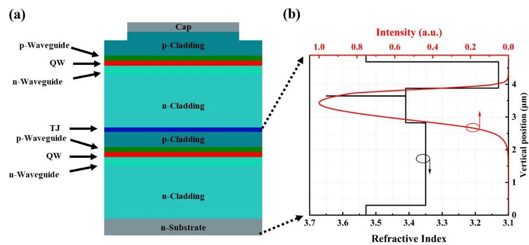
Figure 1. (a) Schematic diagram of the double-junction BAL structure, including substrate, cladding layers, waveguide layer, cap layer, quantum wells (QW), and tunnel junction (TJ). (b) Refractive index distribution and calculated transverse fundamental mode intensity of the single-junction BAL.
We fabricated single-junction and double-junction BALs. The double heterojunction was grown on n-type 6-inch GaAs substrates using metal-organic chemical vapor deposition (MOCVD). Each heterojunction includes a compressively strained InGaAs/AlGaAs quantum well (QW) with an emission wavelength near 915nm. After epitaxial growth, conventional photolithography and wet etching were used to form a 500μm wide injection mesa. Subsequently, a SiO2 insulating layer and p-metal contacts were deposited. Then substrate thinning and N-metalization were performed. Finally, the cavity length of 5.6mm single-chip laser was formed by cleaving. The front and rear cavity facets were passivated and coated with anti-reflection (AR) and high-reflection (HR) coatings, respectively. The laser chip was packaged on a diamond heat sink using indium solder in a p-down configuration.
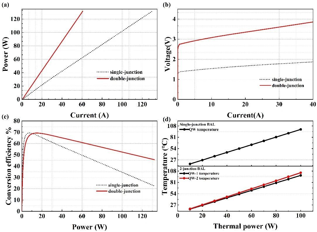
Figure 2. Numerical simulation of output characteristics of single-junction and double-junction BALs. (a) As the number of junctions increases, the required drive current decreases linearly for the same output power. (b) As the number of junctions increases, the turn-on voltage of the BAL also increases linearly. (c) As the number of junctions increases, the PCE peak slightly shifts toward higher power. For higher power, the PCE of double-junction devices increases. (d) Relationship between the active region temperature of the BAL and thermal power.
3. Results and Discussion
Figure 3 shows cross-sectional scanning electron microscope (SEM) images of single-junction and double-junction BALs. The L-I-V results of BALs with different numbers of junctions are shown in Figures 4a and 4b. Obviously, as the current increases, the output power increases almost linearly, and no thermal rollover is observed within the current range. As shown in Figure 4a, the threshold current of the single-junction BAL is 3.5 A, while that of the double-junction BAL is 3.4 A, showing a small difference. The slope efficiency and threshold voltage of the BAL increase proportionally with the number of p-n junctions. The slope efficiency of the double-junction BAL reaches 2.30 W/A, and the threshold voltage is 2.6 V. For the same output power, a higher threshold voltage and lower current are very advantageous because lower current means less Joule heating. When the chip operates at high current injection (the threshold current ratio becomes very small and its effect on optical power can be ignored), the Joule heat of the double-junction device can be reduced by 50%, resulting in higher output power. Figure 4a shows that when the single-junction BAL outputs maximum power of 81 W, the Joule heat generated by the single-junction and double-junction devices is 47.9 W and 36.2 W respectively, corresponding to 37% and 31.4% of the injected power. Meanwhile, the optical power density of the double-junction device is only 0.081 W/μm, half that of the single-junction device, significantly improving device reliability. Excitingly, at a heat sink temperature of 25°C, the peak power of the double-junction BAL exceeds 132.5 W at 70 A current. To the authors' knowledge, this is the highest output power reported for a single BAL device to date. Figure 4b shows that as the number of junctions increases, the peak conversion efficiency slightly decreases from 71.8% to 69.3%. The double-junction device exhibits higher conversion efficiency at higher output power, with efficiencies of 66.7% and 60% at 100 W and 132 W optical power output, respectively.
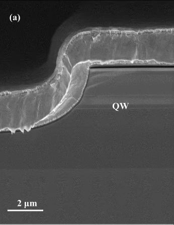
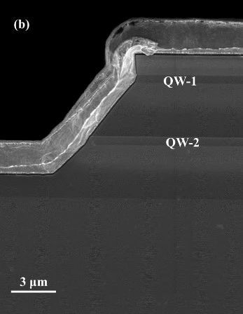
Figure 3. (a) Cross-sectional SEM image of single-junction BAL and (b) cross-sectional SEM image of double-junction BAL.
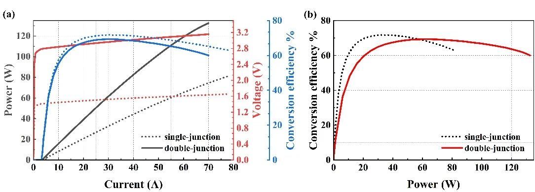
Figure 4. (a) L-I-V results of BALs with different numbers of junctions. The double-junction BAL outputs over 132.5 W at 70 A current and 25°C heat sink temperature. Black line: Power; Blue line: Conversion efficiency; Red line: Voltage. (b) Relationship between power conversion efficiency and output power for BALs with different numbers of junctions.
We used the spectral shift method [24] to evaluate the junction temperature characteristics of the devices, with a spectral shift coefficient of 0.32 nm/K. In Figure 5a, the junction temperatures of single-junction and double-junction devices are presented as a function of output power. When the output power is below 48 W, the single-junction device shows a lower temperature. However, as the output power increases, the temperature rises rapidly. In contrast, the double-junction device has a lower junction temperature at higher currents, consistent with our simulation results. Extrapolating, when the single-junction device outputs 132.5 W, the junction temperature is 89°C, 30°C higher than that of the double-junction device. Higher junction temperature leads to reduced internal quantum efficiency and increased internal losses. Therefore, the optical power gradually saturates, as shown in the L-I curve in Figure 4a. Figure 5b shows the emission spectra of the double-junction BAL at different injection currents. As the injection current increases, the spectrum broadens significantly, especially at 60 A and 70 A injection currents. This result is attributed to the different distances of the two quantum wells from the heat sink, causing the temperature of QW-2 to be slightly higher than QW-1, resulting in offset peak positions and spectral broadening. Additionally, spectral broadening includes carrier Fermi level broadening in each quantum well. Spectral analysis indicates a 1.35 nm difference in peak wavelength between the two active regions at 70 A current, corresponding to a temperature difference of about 4.2°C, consistent with our simulation results. The blue shift of the gain peak during epitaxial growth can suppress spectral broadening.
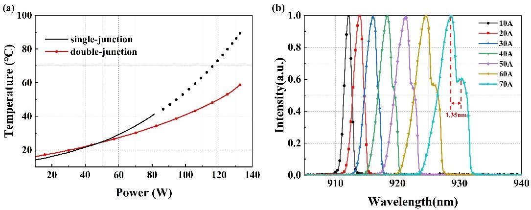
Figure 5. (a) Relationship between junction temperature and output power for BALs with different numbers of junctions. The temperature of the double-junction device is lower than that of the single-junction device. (b) Emission spectra of the double-junction BAL at different injection currents.
We used the slit scanning method to test the near-field distribution of the double-junction BAL at 61 A injection current, as shown in Figure 6a. The near-field profile distribution is uniform, with a width containing 95% of the energy of about 491.5 μm. The near-field CCD image and cavity facet optical microscope photo indicate that the near-field width is almost the same as the current injection width. Although there is slight current spreading in QW-2, it does not extend to the edge of the etched groove. This result proves that current spreading caused by the tunnel junction can be neglected. Figure 6b shows the lateral and transverse far-field distributions at 61 A injection current. The lateral far-field divergence angle containing 95% of the energy is about 12.4°, while the transverse far-field divergence angle is about 51°.
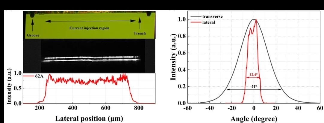
Figure 6. (a) Near-field CCD image, near-field distribution, and cavity facet microscope photo at 61 A injection current. (b) Lateral and transverse far-field distributions at 61 A injection current.
4. Conclusion
We compared the output characteristics of single-junction and double-junction BALs. Simulation results show that at the same output power, the double-junction BAL has nearly half the injection current at room temperature, thereby reducing Joule heating. Therefore, multi-junction BALs provide a new approach to increasing BAL output power. To verify this concept, we fabricated BALs identical to the simulation and conducted a comprehensive analysis of their output characteristics. The results show that the double-junction BAL achieved a maximum DC optical power output of 132.5 W at a heat sink temperature of 25°C. The power conversion efficiencies were 66.7% and 60% at 100 W and 132 W, respectively. Meanwhile, the optical power density was only half that of the single-junction BAL, significantly improving BAL reliability. To our knowledge, this result represents the highest DC continuous output power reported for a single device in the semiconductor laser field.
References
1. Leisher, P.O.; Labrecque, M.; McClune, K.; Burke E., Renner, D., Campbell, J. Origin of the longitudinal current crowding effect in high power diode lasers. In Proceedings of the 2021 27th International Semiconductor Laser Conference (ISLC), Potsdam, Germany, 10–14 October 2021. [M1] [Wu Liu2] IEEE: New York, NY, USA, 2021; pp. 1–2.
2. Arslan , S.; Wenzel, H.; Fricke, J.; Thies, A.; Ginolas, A.; Eppich, B.; Tränkle, G.; Crump, P. Experimental and theoretical studies into longitudinal spatial hole burning as a power limit in high-power diode lasers at 975 nm. Appl. Phys. Lett. 2023, 122, 261101.
3. Arslan, S.; Swertfeger, R.B.; Fricke, J.; Ginolas, A.; Stölmacker, C.; Wenzel, H.; Crump, P.A.; Patra, S.K.; Deri, R.J.; Boisselle, M.C. Non-uniform longitudinal current density induced power saturation in GaAs-based high power diode lasers. Appl. Phys. Lett. 2020, 117, 203506.
4. Todt, R.; Deubert, S.; Jaeggi, D. High-volume manufacturing of state-of-the-art high-power laser diodes on 6-inch GaAs. In Proceedings of the High-Power Diode Laser Technology XX, San Francisco, CA, USA, 22 January–28 February 2022; SPIE: Bellingham, WA, USA, 2022; Volume 11983, pp. 11–19.
5. Wang, J.; Smith, B.; Xie, X.; Wang, X.; Burnham, G.T. High-efficiency diode lasers at high output power. Appl. Phys. Lett. 1999, 74, 1525–1527.
6. Miah, M.J.; Strohmaier, S.; Urban, G.; Bimberg, D. Beam quality improvement of high-power semiconductor lasers using laterally inhomogeneous waveguides. Appl. Phys. Lett. 2018, 113, 221107.
7. Boni, A.; Arslan, S.; Erbert, G.; Della Casa, P.; Martin, D.; Crump, P. Epitaxial design progress for high power, efficiency, and brightness in 970 nm broad area lasers. In Proceedings of the High-Power Diode Laser Technology XIX, Online, 6–12 March 2021; SPIE: Bellingham, WA, USA, 2021; Volume 11668, pp. 15–22.
8. Campbell, J.; Labrecque, M.; Foong, F.; Renner, D.; Mashanovitch, M.; Leisher, P. Watt-class, COMD-free ridge waveguide lasers at 885 nm. In Proceedings of the 2021 27th International Semiconductor Laser Conference (ISLC), Potsdam, Germany, 10–14 October 2021; IEEE: New York, NY, USA, 2021; pp. 1–2.
9. Crump, P.; Elattar, M.; Miah, M.J.; Ekterai, M.; Karow, M.M.; Martin, D.; Della Casa, P.; Maaßdorf, A.; McDougall, S.; Holly, C.; et al. Progress in experimental studies into the beam parameter product of GaAs-based high-power diode lasers. In Proceedings of the High-Power Diode Laser Technology XX, San Francisco, CA, USA, 22 January–28 February 2022; SPIE: Bellingham, WA, USA, 2022; Volume 11983, pp. 43–52.
10. King, B.; Arslan, S.; Boni, A.; Basler, P.S.; Zink, C.; Della Casa, P.; Martin, D.; Thies, A.; Knigge, A.; Crump, P. GaAs-based wide-aperture single emitters with 68 W output power at 69% efficiency realized using a periodic buried-regrown-implant structure. In Proceedings of the European Conference on Lasers and Electro-Optics, Munich, Germany, 26–30 June 2023; Optica Publishing Group: [M3] [Wu Liu 4], Washington, DC, USA, 2023; p. cb_11_1.
11. Wang, B.; Tan, S.; Zhou, L.; Zhang, Z.; Xiao, Y.; Liu, W.; Gou, Y.; Deng, G.; Wang, J. High Reliability 808nm Laser Diodes with Output Power Over 19W Under CW Operation. IEEE Photonics Technol. Lett. 2022, 34, 349–352.
12. Miah, M.J.; Boni, A.; Martin, D.; Della Casa, P.; Crump, P. Highly asymmetric epitaxial designs for increased power and efficiency in kW-class gaas-based diode laser bars. In Proceedings of the 2021 27th International Semiconductor Laser Conference (ISLC), Potsdam, Germany, 10–14 October 2021; IEEE: New York, NY, USA, 2021; pp. 1–2.
13. Crump, P.; Grimshaw, M.; Wang, J.; Dong, W.; Zhang, S.; Das, S.; Farmer, J.; DeVito, M.; Meng, L.S.; Brasseur, J.K.; et al. 85% power conversion efficiency 975-nm broad area diode lasers at −50 C, 76% at 10 C. In Proceedings of the 2006 Conference on Lasers and Electro-Optics and 2006 Quantum Electronics and Laser Science Conference, Long Beach, CA, USA, 21–26 May 2006; IEEE: New York, NY, USA, 2006; pp. 1–2.
14. Petrescu-Prahova, I.B.; Modak, P.; Goutain, E.; Bambrick, D.; Silan, D.; Riordan, J.; Moritz, T.; Marsh, J.H. 253 mW/μm maximum power density from 9xx nm epitaxial laser structures with d/Γ greater than 1 μm. In Proceedings of the 2008 IEEE 21st International Semiconductor Laser Conference, Sorrento, Italy, 14–18 September 2008; IEEE: New York, NY, USA, 2008; pp. 135–136.
15. Gapontsev, V.; Moshegov, N.; Berezin, I.; Komissarov, A.; Trubenko, P.; Miftakhutdinov, D.; Berishev, I.; Chuyanov, V.; Raisky, O.; Ovtchinnikov, A. Highly-efficient high-power pumps for fiber lasers. In Proceedings of the High-Power Diode Laser Technology XV, San Francisco, CA, USA, 28 January–2 February 2017; SPIE: Bellingham, WA, USA, 2017; Volume 10086, pp. 16–25.
16. Liu, Y.; Yang, G.; Zhao, Y.; Tang, S.; Lan, Y.; Zhao, Y.; Demir, A. 48 W continuous-wave output from a high-efficiency single emitter laser diode at 915 nm. IEEE Photonics Technol. Lett. 2022, 34, 1218–1221.
17. Tan, S.; Liu, W.; Wang, B.; Zhao, W.; Wang, J. Lateral brightness improvement of high-power semiconductor laser diode. In Proceedings of the High-Power Diode Laser Technology XXI, San Francisco, CA, USA, 28 January–3 February 2023; SPIE: Bellingham, WA, USA, 2023; Volume 12403, pp. 223–228.
18. Gou, Y.; Wang, H.; Wang, J.; Yang, H.; Deng, G. High performance p++-AlGaAs/n++-InGaP tunnel junctions for ultra-high concentration photovoltaics. Opt. Express 2022, 30, 23763–23770.
19. Aboujja, S.; Chu, D.; Bean, D. 1550nm triple junction laser diode for long range LiDAR. In Proceedings of the High-Power Diode Laser Technology XX, San Francisco, CA, USA, 22 January–28 February 2022; SPIE: Bellingham, WA, USA, 2022; Volume 11983, pp. 196–207.
20. Ammouri, N.; Christopher, H.; Maassdorf, A.; Fricke, J.; Ginolas, A.; Liero, A.; Wenzel, H.; Knigge, A.; Traenkle, G. Distributed feedback broad area lasers with multiple epitaxially stacked active regions and tunnel junctions. Opt. Lett. 2023, 48, 6520–6523.
21. Choi, A.; Park, J.; Lee, J.; Kim, Y.; Kim, T. 905nm 140W pulse laser diode with 4Stack epitaxy structure for autonomous lidar. In Proceedings of the High-Power Diode Laser Technology XXI, San Francisco, CA, USA, 28 January–3 February 2023; SPIE: Bellingham, WA, USA, 2023; Volume 12403, pp. 37–43.
22. Wenzel, H.; Maaßdorf, A.; Zink, C.; Martin, D.; Weyers, M.; Knigge, A. Novel 900 nm diode lasers with epitaxially stacked multiple active regions and tunnel junctions. Electron. Lett. 2021, 57, 445–447.
23. Xiao, Y.; Wang, J.; Liu, H.; Miao, P.; Gou, Y.; Zhang, Z.; Deng, G.; Zhou, S. Multi-junction cascaded vertical-cavity surface-emitting laser with a high power conversion efficiency of 74%. Light. Sci. Appl. 2024, 13, 60.
24. Siegal, B. Laser diode junction temperature measurement alternatives: An overview. In Proceedings of the PhoPack, Stanford, CA, USA, 14–16 July 2002.
[M1]Newly added information. Please confirm. The following highlights are the same.
Recommended Reading

Address: No.56,Lijiang Road,SND,Suzhou,Jiangsu Province,P.R.China
Mailbox:sales@everbrightphotonics.com
Website:www.everbrightphotonics.com
Phone:+86 0512-66896988
Fax:+86 0512-66806323
Message Board