


Research on High-Performance Multi-Junction VCSEL Chips for LiDAR
07/04
2022
Heng Liu a,b , Pei Miao a,b , Yao Xiao a,b , Chang Liu a,b , Zhicheng Zhang a,b , and Jun Wang a,b,*a Suzhou Everbright Photonics Co., LTD, Suzhou, Jiangsu, P. R. China b Sichuan University, Chengdu, Sichuan, P. R. China
Liu Heng a,b , Miao Pei a,b , Xiao Yao a,b , Liu Chang a,b ,
Zhang Zhicheng a,b , Wang Jun a,b,*
a Suzhou Everbright Photonics Co., LTD,
Suzhou
b Sichuan University, Chengdu
Proceedings Volume 12020, Vertical-Cavity Surface-Emitting Lasers XXVI; 1202005 (2022) https://doi.org/10.1117/12.2609601Event: SPIE OPTO, 2022, San Francisco, California, United States
Abstract
In the field of LiDAR applications, high power density vertical-cavity surface-emitting lasers (VCSELs) have attracted increasing attention. Multi-junction VCSELs are a key technology to achieve high power density. To obtain high-performance multi-junction VCSEL arrays, high slope efficiency, high fill factor, and small divergence angle are the main research directions. We optimized epitaxial design and fabrication processes, such as tunnel junctions, oxide layers, and array layout. This paper reports high-performance multi-junction VCSEL arrays with lasing wavelengths near 940nm. As the basic light source for LiDAR applications, selectively oxidized front-emitting VCSEL arrays have been realized, featuring 59.7% photoelectric conversion efficiency and 8.3 W/A slope efficiency. The processed VCSEL array device has an emission area of 234*250um 2 , 15A peak current, 10KHz 10ns (FWHM) pulse width test conditions, power density greater than 1800W/mm 2 . Divergence angle less than 21 degrees (1/e 2 ).
Keywords: LiDAR, vertical-cavity surface-emitting laser array, multi-junction, high power density, small divergence angle
01 Background Introduction
In recent years, with the development of LiDAR technology, VCSEL array light sources have attracted increasing attention in the LiDAR application market due to their low manufacturing cost, small temperature drift coefficient, and ease of two-dimensional integration. Firstly, using special structures and process designs, VCSEL arrays can achieve higher power density and lower divergence angle to meet the development needs of long-distance LiDAR applications. Utilizing multi-junction VCSEL technology is key to achieving higher efficiency and higher power density. Secondly, using special structural designs, such as optimizing the position, thickness, and Al composition of the oxide layer, divergence performance can be further optimized. Finally, a higher fill factor means a smaller chip area, which also benefits higher output power density. Considering nanosecond-level short pulse test conditions, thermal accumulation in VCSEL arrays can be neglected. Large oxide apertures and small pitch sizes can also be used to improve the fill factor.
In this paper, by optimizing epitaxial structure design and manufacturing processes, VCSEL arrays can achieve high power density and low divergence angle. Under wafer-level 100Hz 10us wide pulse test conditions, the energy conversion efficiency peak of the VCSEL array reaches 59.7%, and the slope efficiency reaches 8.3 W/A. Additionally, under device-level 10KHz 10ns short pulse test conditions, the VCSEL array can achieve peak power output exceeding 110W, corresponding to a power density higher than 1800W/mm 2 , with a divergence angle reaching 21°.
02 High Beam Quality Multi-Junction VCSEL Array Design
2.1 Application Requirements
LiDAR is a technology that uses laser imaging to perform precise distance measurements and is considered one of the most important detection technologies in fields such as intelligent driving and 3D sensing. As the detection distance increases, the point cloud density decreases, and resolution is also limited. To achieve long-distance 3D scanning reconstruction, a high-quality laser beam with higher power density and lower divergence angle is required.
The design concept is shown in Figure 1. Using nanosecond short pulse testing, multi-junction VCSEL arrays with small divergence angles provide an excellent platform for LiDAR applications. Based on this concept, we designed and manufactured world-leading multi-junction VCSEL arrays (5/6/8 junctions) and used special oxide layer and fill factor designs to achieve higher power density and lower divergence angle performance.
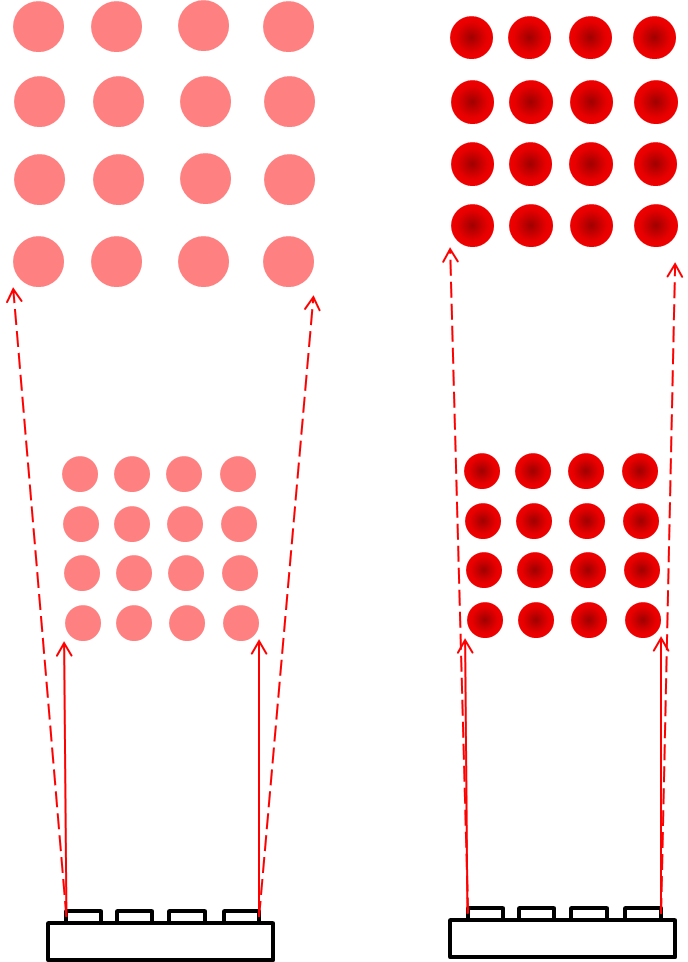
Figure 1. LiDAR light source detection schematic, left is conventional, right is optimized result with higher power density and smaller divergence angle.
2.2 Device Photoelectric Performance
2.2.1 Efficiency Optimization
To improve power conversion efficiency (PCE) and slope efficiency (SE), the gain volume of the device can be increased by stacking multiple active regions. In our multi-junction structure design, we utilized low series resistance, low absorption tunnel junction design, and precise control of epitaxial layer thickness to align the gain medium with the gain optical field. The structural schematic and equivalent circuit diagram of the 6-junction VCSEL array are shown in Figure 2.
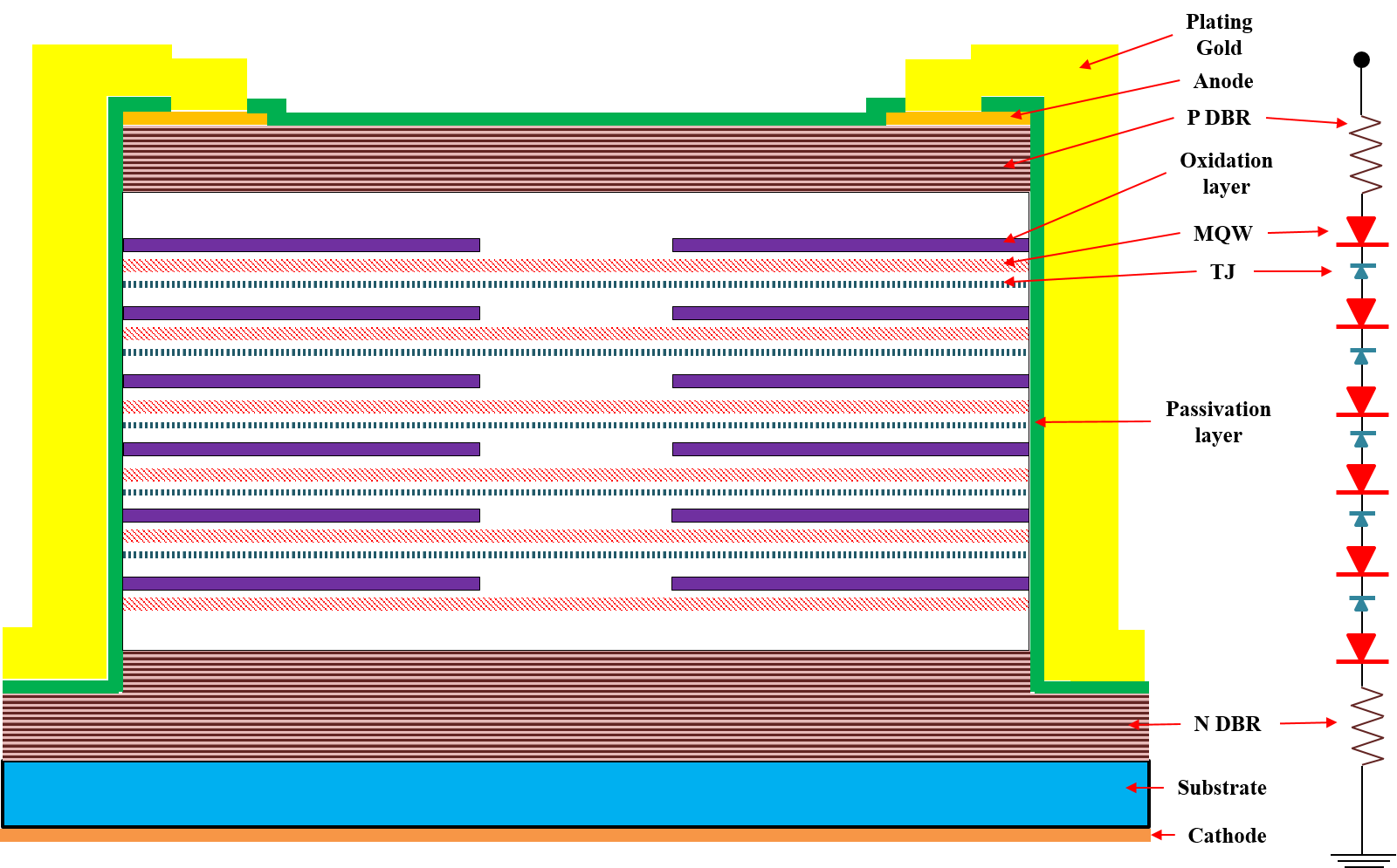
Figure 2. Structural schematic and equivalent circuit model of the 6-junction VCSEL.
2.2.2 Divergence Angle Optimization
For traditional multi-junction VCSEL arrays, the divergence angle increases with the number of tunnel junctions and quantum wells. Based on literature reports and our simulation results, the divergence angle of the VCSEL array is influenced by oxidation layer parameters such as position, thickness, Al composition, and quantity, as shown in Figure 3. Figure 3a presents the structural schematic of a traditional 6-junction VCSEL. The aforementioned oxidation layer parameters affect the effective refractive index difference between the "core" (central region) and the "cladding" (oxidized region). Additionally, different gain-loss ratios at various positions are introduced, causing changes in the distribution positions of the fundamental transverse mode and higher-order transverse modes. Expanding the proportion of the fundamental transverse mode is beneficial for optimizing the divergence angle.
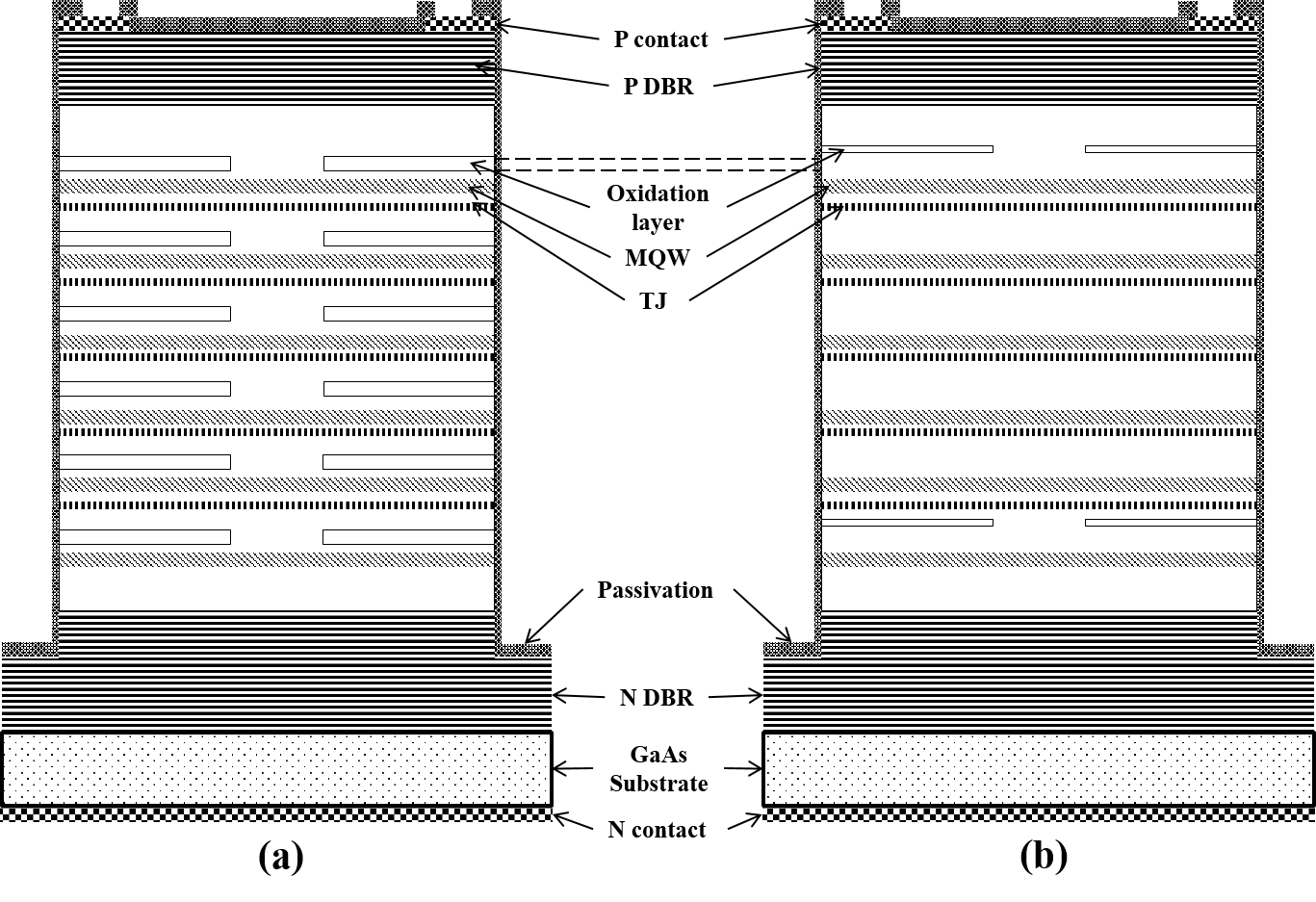
Figure 3. Divergence angle optimization mechanism. (a) Structural diagram of a traditional 6-junction VCSEL, (b) optimized structure for divergence angle performance.
2.2.3 Filling factor optimization
The filling factor is defined as the total light-emitting window area divided by the total light-emitting area. The total light-emitting window area depends on the oxidation aperture of each emission hole, and the total light-emitting area depends on the outer diameter of the beam array.

Formula 1
Where F is the filling factor, r is the radius of the oxidation aperture, and N is the number of emission points, A L is the length of the total light-emitting area, A w is the width of the total light-emitting area.

Formula 2
Where J is the current density, I o is the operating current.
From formulas 1 and 2, for a given total light-emitting area, a low filling factor leads to higher current density, causing the device to operate in a high current density mode. In this mode, the likelihood of damage increases, affecting device reliability. Secondly, high current density more easily causes gain saturation, which, although below the actual operating current of LiDAR, also affects conversion efficiency and slope efficiency. Thirdly, a high filling factor reduces device series resistance, providing more room for voltage limits of the driver circuit board. We adjusted the size of the oxidation aperture, mesa size, and the period of the emission array to achieve a VCSEL array layout with a high filling factor, as shown in Figure 4c. In Figure 4, from a, b to c, the filling factors are 27.0%, 42.0%, and 48.8%, respectively.
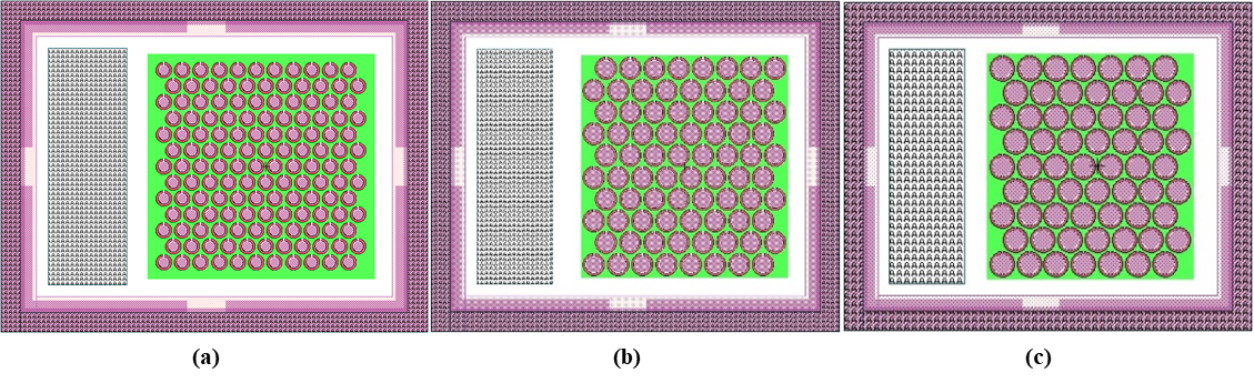
Figure 4. Filling factor optimization mechanism. a) Layout design with a filling factor of 27.0%, b) layout design with a filling factor of 42.0%, c) layout design with a filling factor of 48.8%.
2.3 Process fabrication
The fabrication process is shown in Figure 5.
a. GaAs Epitaxial growth on the substrate.
b. Stress compensation of Ti and SiN on the backside. P-type contact metal is deposited on the surface of the p+ metal layer.
c. Dry etching to form the mesa.
d. Oxidation process in the oxidation furnace tube.
e. PECVD Growth of SiN passivation layer.
f. ICP-RIE Etching to form current injection vias.
g. Seed metal deposition and gold electroplating for current injection.
h. After polishing the substrate, N-type contact metal is deposited on the N side.
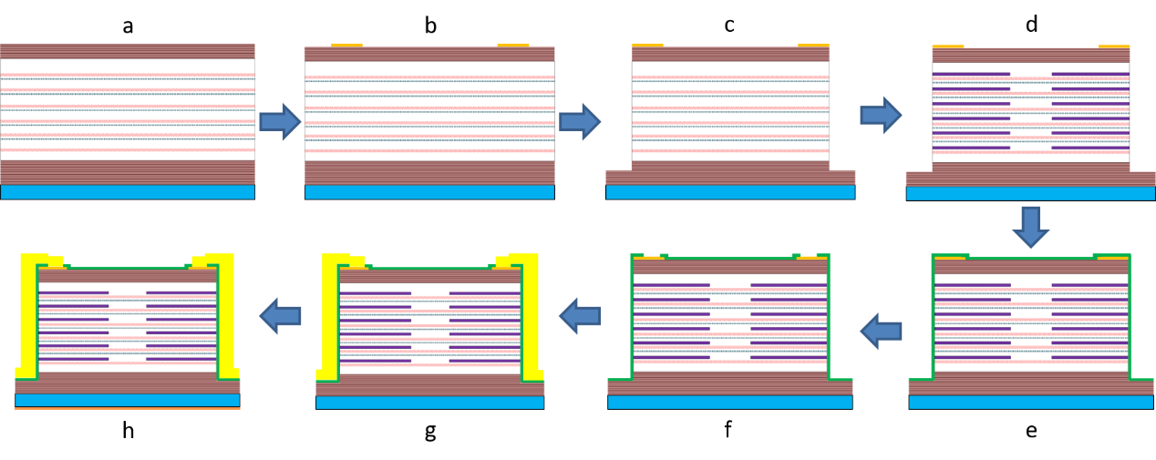
Figure 5. Process flow diagram.
03 Discussion of results from different designs
3.1 High efficiency
We completed the fabrication process for 5/6/8-junction VCSEL arrays. Figure 6 shows the comparison of 5/6/8-junction VCSEL arrays driven by 100Hz 10us pulse current. With the increase in the number of junctions, the slope efficiency increased from 4.9 W/A to 5.9 W/A, and finally to 8.3 W/A, as shown in Figure 6a. The maximum conversion efficiency increased from 48.7% to 56.5%, and finally to 59.7%, as shown in Figure 6b.
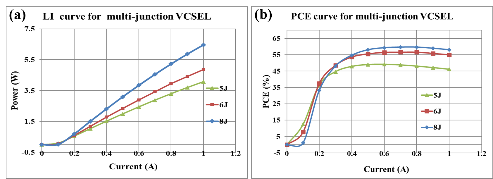
Figure 6. LI and PCE curves of 5/6/8-junction VCSEL arrays driven by 100Hz 10us pulse current. a) LI curve, b) PCE curve.
3.2 Low divergence angle
To demonstrate the divergence angle optimization design based on different oxidation layer positions, we increased the waveguide layer thickness to ensure the optical distance between the oxidation layer and the active region is 0.25lambda, 0.75lambda, and 1.25lambda. As shown in Figure 7, under 10kHz 10ns short pulse test conditions, the divergence angles were optimized to 27.9°, 26.6°, and 24.6°, respectively.
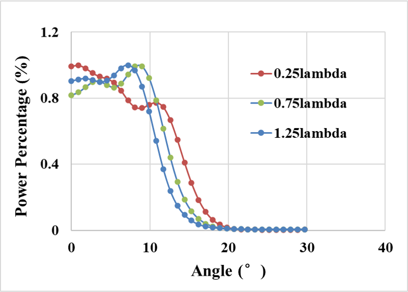
Figure 7. Effect of different oxidation layer positions on divergence angle under short pulse driving.
3.3 High filling factor
For the three structures a/b/c in Figure 4, we fabricated 5-junction VCSEL arrays. Different oxidation apertures were realized based on different mesa sizes. Considering the given VCSEL array layout, Figure 8a shows the LI curves for oxidation apertures of 8um/10um/12um. Under 10kHz 10ns short pulse test conditions, using a small oxidation aperture such as 8um results in reduced slope efficiency due to relatively high current density. Additionally, the LI curves of A, B, and C structures designed for different filling factors are shown in Figure 8b. Within a certain range, slope efficiency increases with the filling factor.
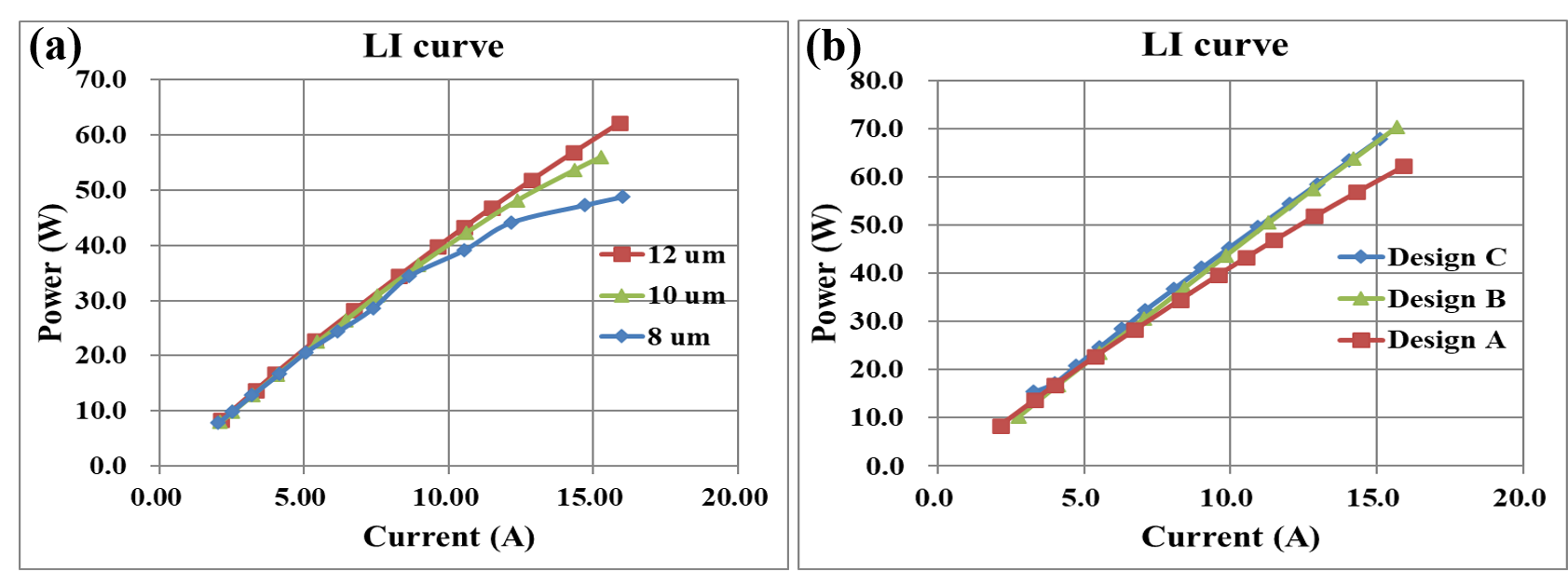
Figure 8. Comparison of LI performance for different filling factor designs. a a) LI curves for different oxidation aperture sizes, b) LI curves for filling factor layout designs A, B, and C.
04 High-performance 8-junction VCSEL array and high-volume production capability
4.1 Performance of optimized 8-junction VCSEL array
Based on the above optimization mechanisms, we realized an 8-junction VCSEL array with high power density, high slope efficiency, and low divergence angle. The performance test conditions were 10kHz 10ns short pulse testing. As shown in Figure 9a, at a driving current of 15A, the total output power was 112W, with a power density exceeding 1800W/mm 2 , and a conversion efficiency of 21%. Meanwhile, its far-field distribution is shown in Figure 9c, and the divergence angle performance is shown in Figure 9d, less than 21°.
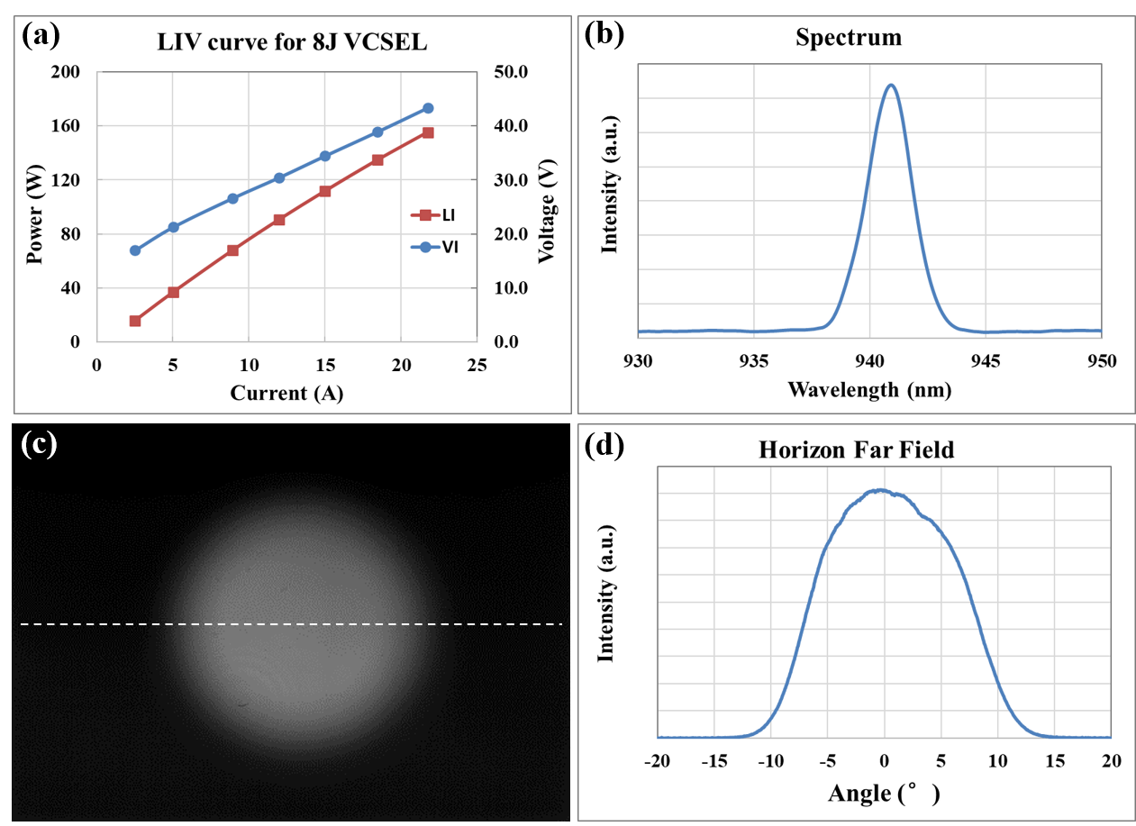
Figure 9. Short pulse test performance of the 8-junction VCSEL array. a ) LIV curve, b) spectral curve, c) CCD image of far-field spot, d) far-field spot intensity distribution.
Considering the nanosecond test conditions, thermal accumulation of the device can be ignored. To study the array performance at different temperatures, we used a TEC to provide ambient temperatures from 30°C to 80°C. In the 10kHz 10ns short pulse test, LI, FF, and spectral performance are shown in Figure 10. Figure 10a demonstrates the extremely high stability of the 8-junction VCSEL array. Under the operating condition of 15A, its power fluctuation range is less than 8%, as shown in Figure 10b. The wavelength drift curve with temperature is shown in Figure 10c, with a coefficient of 0.07nm/°C, as shown in Figure 10d.
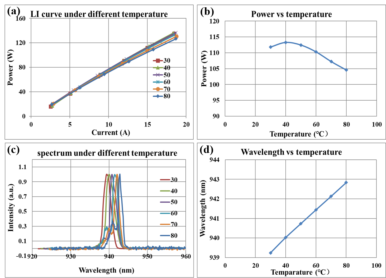
Figure 10. Temperature-dependent performance of the 8-junction VCSEL array. a ) LI curves at different temperatures, b) power variation with temperature, c) spectral variation with temperature, d) wavelength drift versus temperature.
4.2 VCSEL High-volume production capability of the chip
Target LiDAR product, Figure 11 shows the uniformity of energy conversion efficiency and wavelength distribution on a 6-inch wafer, demonstrating the excellent mass production control capability of Suzhou Changguang Huaxin Optoelectronics Technology Co., Ltd.'s 6-inch production line. Figure 11a indicates that over 95% of devices in working condition have energy conversion efficiencies between 54% and 58%. Figure 11b shows that over 95% of devices in working condition have wavelength distributions between 935nm and 945nm.
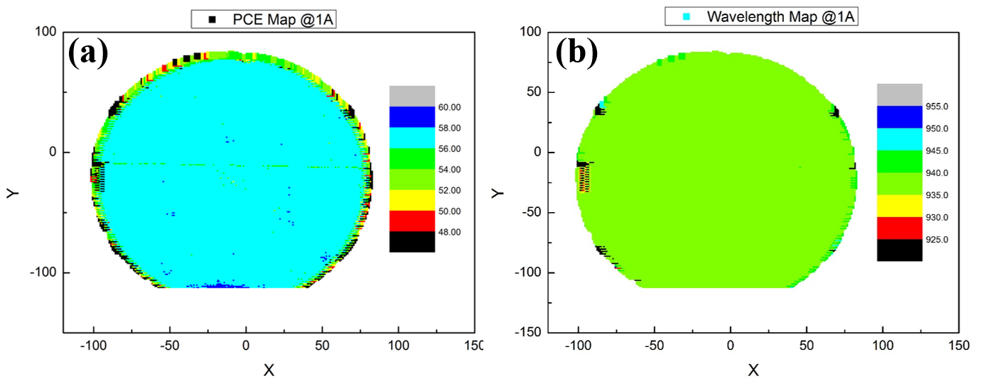
Figure 11. Uniformity of the 6-inch wafer VCSEL array. a ) PCE Map, b) Wavelength Map.
5 Summary
This paper designs and manufactures a multi-junction VCSEL array with high energy density and low divergence angle for LiDAR applications. The optimized maximum energy conversion efficiency is 59.7%, with a slope efficiency of 8.3W/A. The test conditions were 100Hz 10μs wide pulse drive. For the 8-junction VCSEL array product, under 10kHz 10ns short pulse drive with a working current of 15A, its power density reaches 1800W/mm 2 , and the divergence angle is less than 21° (1/e 2 ). Custom services can be provided according to customer requirements for wavelength, energy density, divergence angle, and other main performance parameters.
Acknowledgments
The authors thank the VCSEL team of Suzhou Changguang Huaxin Optoelectronics Technology Co., Ltd. for their work in device design, wafer fabrication, packaging, and testing.
References
[1] Kim, I., Martins, R. J., Jang, J., and et al, “Nanophotonics for light detection and ranging technology,” Nature Nanotechnology 16, 508–524 (2021). [2] Moench, H., Carpaij, M., Gerlach, P., Gronenborn, S., Gudde, R., Hellmig, J., Kolb, J., and v.d. Lee, A., “VCSEL based sensors for distance and velocity,” Proc. of SPIE 9766, 97660A (2016). [3] Zhou, D., Zhao, B., Fan, Y., Chong, H., Wang, G., Wang, P., Yuan, K., Li, L., en Zah, C., and Liu, X., “Research on VCSEL transmitter modules for intelligent driving,” Proc. SPIE 11891, 118910S (2021). [4] Warren, M. E., Podva, D., Dacha, P., Block, M. K., Helms, C. J., Maynard, J., and Carson, R. F., “Low divergence high-power VCSEL arrays for LiDAR application,” Proc. SPIE 10552, 105520E (2018).[5] Moench, H., Gronenborn, S., Gu, X., Gudde, R., Herper, M., Kolb, J., Miller, M., Smeets, M., and Weigl, A., “VCSELs in short-pulse operation for time-of-flight applications,” Proc. SPIE 10552, 105520G (2018). [6] Yuen, A., Barvem, A. V., Zhao, G., and Hegblom, E. R., “Controlling beam divergence in a vertical-cavity surface-emitting laser,” United States Patent Application Publication , US 2019/0067906 A1 (2019).
Recommended Reading

Address: No.56,Lijiang Road,SND,Suzhou,Jiangsu Province,P.R.China
Mailbox:sales@everbrightphotonics.com
Website:www.everbrightphotonics.com
Phone:+86 0512-66896988
Fax:+86 0512-66806323
Message Board