


Cutting-edge Technology | Semiconductor Lasers and Laser Cells for Optical Wireless Power Transmission
05/12
2023
On April 19, Dr. Jun Wang, CTO of Changguang Huaxin, was invited to give an academic report titled "Semiconductor laser and power converter for optical wireless power transmission" at the OPTICS & PHOTONICS International Congress 2023 (OPIC2023). The report detailed the latest progress of the transmitting laser chips and modules, receiving single-junction/multi-junction laser cell chips and modules, and laser wireless power transfer systems used for laser wireless energy transmission (808 nm and 1 μm). This includes: an 808 nm laser chip with an output power of 19W@100μm, a 780 nm laser chip with an electro-optical conversion efficiency of 70%, a 3000 W fiber-coupled laser module; a six-junction laser cell chip with a photoelectric conversion efficiency of 70.1%, output power of 15.45 W, and chip size of 40.7 mm*45.1 mm, and a 20m laser wireless power transfer demonstration system with an output power of 179W. Also included are a 9xx nm laser chip with an output power of 51 W@230μm, a 1 μm laser module with an output power of 600 W; and a lattice-mismatched 1 μm laser cell chip with a photoelectric conversion efficiency of 40.1%.
This report is the first domestic and international report on a fully semiconductor, fully independent, full-link laser wireless energy transmission chip, which has received high praise from peers at home and abroad and caused a strong response.
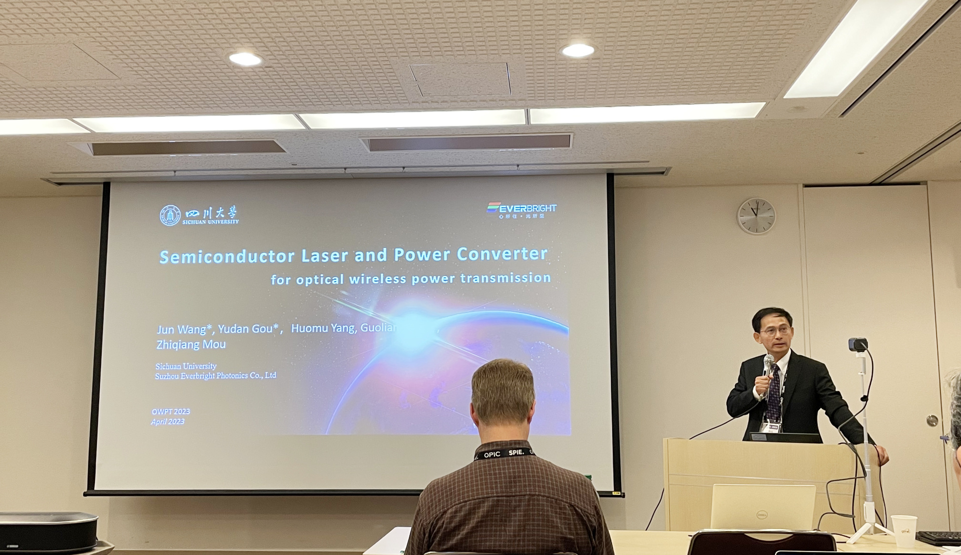
Chinese translation of the report ▼
Semiconductor laser and power converter for optical wireless power transmission
Semiconductor laser and laser cell for optical wireless energy transmission
Jun Wang a,b* ,Yudan Gou a,b* , Huomu Yang a , Guoliang Deng a , Zhiqiang Mou a
a Sichuan University, Chengdu, P.R. China
b Suzhou Everbright Photonics Co., Ltd., Suzhou, P.R. China
Jun Wang a,b* Yudan Gou a,b* Huomu Yang a Guoliang Deng a Zhiqiang Mou a
a Sichuan University, Chengdu
b Suzhou Changguang Huaxin Optoelectronics Technology Co., Ltd., Suzhou
Abstract
Laser wireless energy transmission technology uses laser as a carrier to achieve wireless transmission of electrical energy in free space. This paper reports the latest progress of transmitting laser chips and modules, receiving single/multi-junction laser cell chips and modules, and laser wireless power transfer systems used for laser wireless energy transmission (808 nm and 1 μm). This includes: an 808 nm laser chip with an output power of 19W@100μm, a 780 nm laser chip with an electro-optical conversion efficiency of 70%, a 3000 W fiber-coupled laser module; a six-junction laser cell chip with a photoelectric conversion efficiency of 70.1%, output power of 15.45 W, and chip size of 40.7 mm*45.1 mm, and a 20m laser wireless power transfer demonstration system with an output power of 179W. Also included are a 9xx nm laser chip with an output power of 51 W@230μm, a 1 μm laser module with an output power of 600 W; and a lattice-mismatched 1 μm laser cell chip with a photoelectric conversion efficiency of 40.1%.
1.0 Introduction
Laser wireless energy transmission technology has the advantages of high energy density and long-distance transmission. It can provide continuous power supply/recharging for in-orbit satellites, drones, mobile terminals, and other equipment as shown in Figure 1, with broad application prospects.
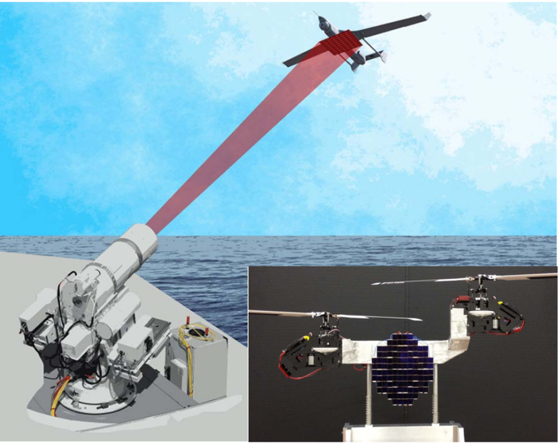
Figure 1 Laser wireless energy transmission applied to continuous power supply/recharging of drones (drone image sourced from the internet)
The laser wireless energy transmission system mainly consists of a laser system at the transmitting end and a laser cell system at the receiving end. The electro-optical characteristics of the transmitting laser chip and module, and the photoelectric characteristics of the receiving laser cell chip and module are key factors affecting the output characteristics of the laser wireless energy transmission system. [3, 4]. Based on this, considering the transmittance characteristics of laser transmission in the atmosphere, as shown in Figure 2, this paper reports the latest progress of 808 nm and 1 μm transmitting and receiving chips and modules, as well as the application of laser wireless energy transmission systems.
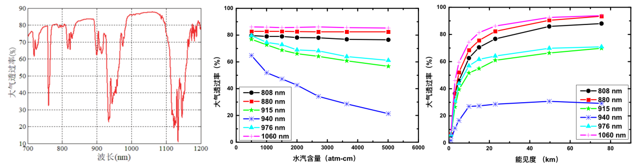
Figure 2 Penetration characteristics of laser transmission in the atmosphere (Image source: Guoxing Hu, Laser ground-to-air transmission calculation; 4th Wireless Power Transfer and Energy Interconnection Technology Forum)
2.1 808 nm laser chip and module
Figure Figure 3 shows the LIV characteristics of 808 nm and 780 nm laser chips using GaInP/GaAsP aluminum-free active region LOC structure laser chips, with optimized doping and waveguide thickness to reduce resistance and internal loss. The output power of the 808 nm laser chip is 19W@100μm, which is the highest power reported for 808 nm to date. The output power of the 780 nm laser chip reaches 120W with an efficiency of 70%, the highest efficiency at this wavelength so far.
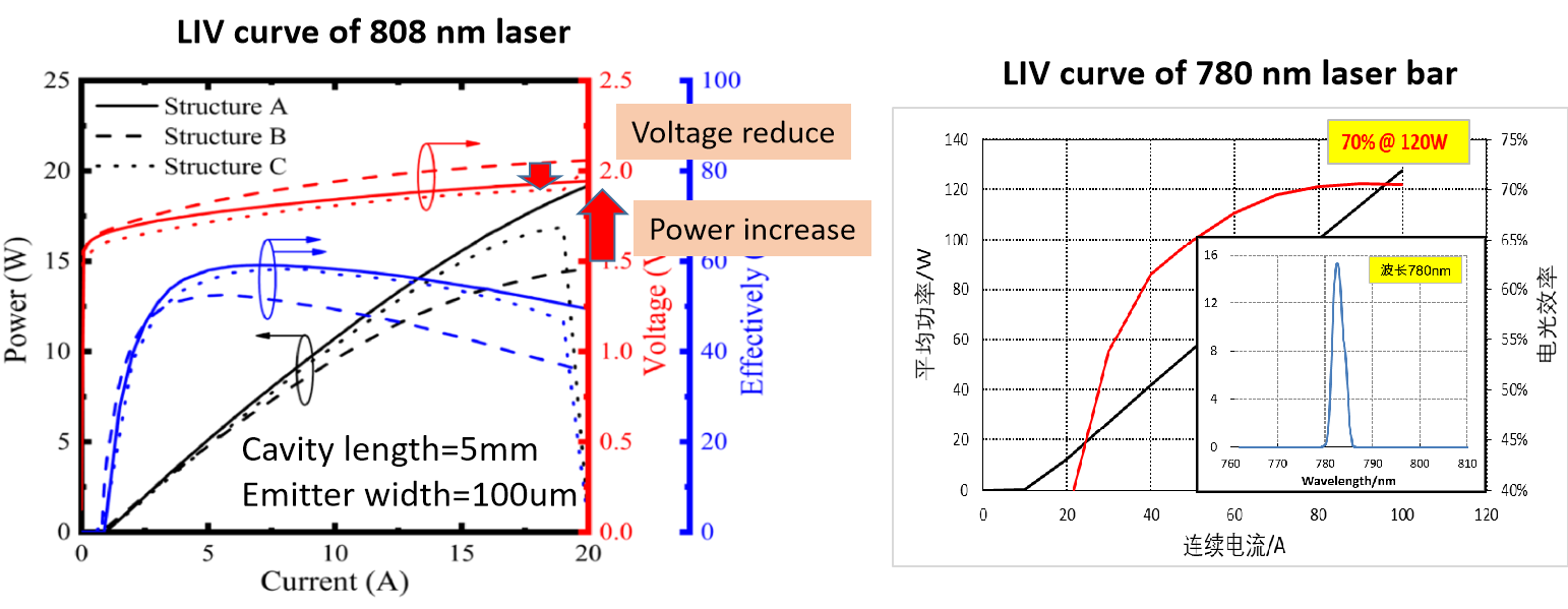
Figure 3 LIV characteristics of 808 nm and 780 nm laser chips
We fabricated an 808 nm fiber-coupled module using polarization beam combining, with an output power of 150W, fiber core diameter of 135 μm/0.22NA, and spectral width less than or equal to 5nm, as shown in Figure 4 and Table 1.
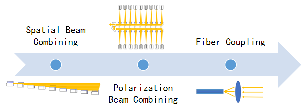

Figure 4 Schematic of 808 nm 150W 135 μm/0.22NA fiber-coupled module polarization beam combining, LIV, spectrum
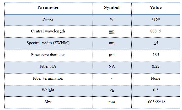
Table 1 Characteristic parameters of 808 nm 150W 135 μm/0.22NA fiber-coupled module
We fabricated an 808 nm laser free-space emission module, as shown in Figure 5, using spatial beam combining, outputting 1kW laser power, with the laser beam propagating 20m to form a square spot with a spot non-uniformity less than 0.271.
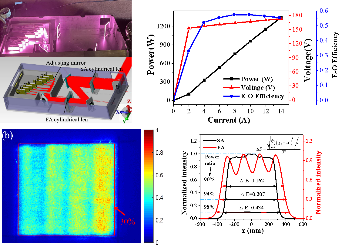
Figure 5 1kW 808 nm Free-Space Laser Emission System
We also prepared a 3000W fiber-coupled laser module using polarization beam combining, with a fiber core diameter of 600μm/0.22NA and spectral width less than or equal to 10nm. The results are shown in Figure 6 and Table 2.
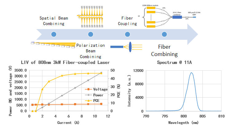
Figure 6 808 nm 3000W 600μm/0.22NA Fiber-Coupled Module Polarization Beam Combining Diagram, LIV, Spectrum
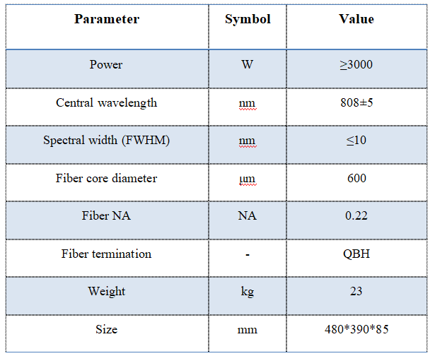
Table 2 808 nm 3000W 600μm/0.22NA Fiber-Coupled Module Characteristic Parameters
2.2 808nm Laser Photovoltaic Cell Chips and Modules
At the receiving end, a tunneling peak current density of 1867 A/cm 2 , a tunneling resistivity of 6.9×10 -5 Ω cm 2 of p++-AlGaAs/n++-AlGaAs tunnel structure vertically series-connected multi-absorption regions. As shown in Figure 7, a multi-junction structure is formed.
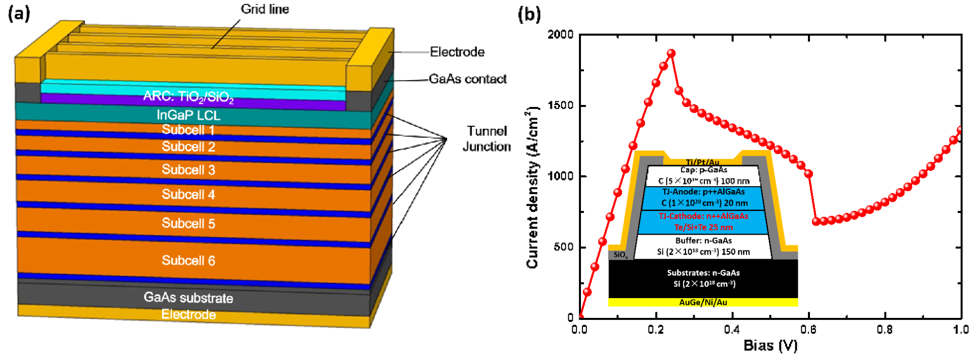
Figure 7 (a) Schematic diagram of the six-junction GaAs laser photovoltaic cell structure. (b) Experimental results of the p++-AlGaAs/n++-AlGaAs tunnel junction device, with the inset showing the tunnel junction structure schematic [5].
We grew and fabricated laser photovoltaic cell chips and modules with different areas and junction numbers. Their typical photoelectric characteristics are shown in Figure 8. The six-junction laser photovoltaic cell achieved a maximum photoelectric conversion efficiency of 70.1%, a maximum output power of 15.45 W, and a maximum chip area of 40.7 mm*45.1 mm.
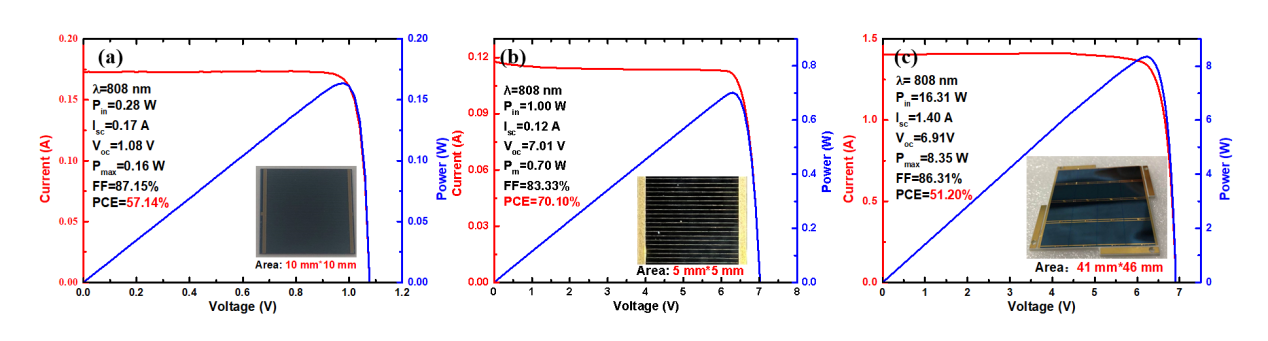
Figure 8 (a) Single-junction GaAs laser photovoltaic cell device performance; (b) Six-junction GaAs laser photovoltaic cell device performance; (c) Large-area six-junction GaAs laser photovoltaic cell device performance
We conducted reliability testing on this laser photovoltaic cell, as shown in Figure 9, where stable output was maintained for 550 hours without degradation under 22.9W laser irradiation.
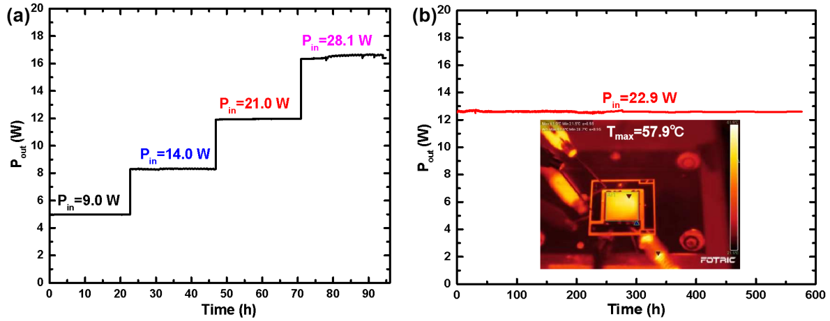
Figure 9 Six-junction GaAs Laser Photovoltaic Cell Reliability Test
2.3 808nm Laser Wireless Power Transmission Demonstration System
We built a kilowatt-level 808 nm laser wireless power transmission system. As shown in Figure 10, a 1 kW laser beam was transmitted 20m and irradiated on a 49×44 cm 2 dense array of laser photovoltaic cells [7], with the receiving end output power reaching 179W. In the future, we will further optimize the receiving end to improve its output characteristics, including enhancing array heat dissipation capability and online circuit control based on dynamic laser spot distribution.
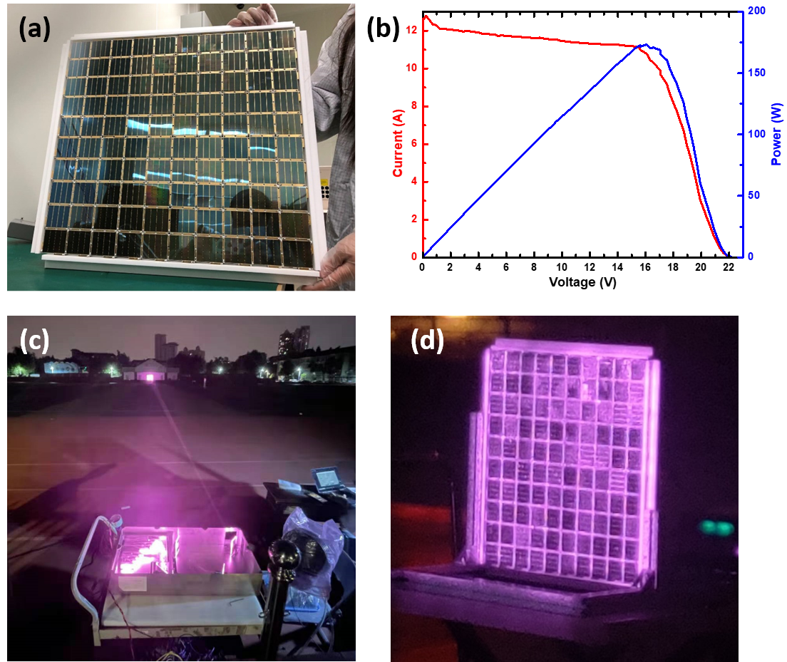
Figure 10 808nm Laser Wireless Power Transmission Demonstration System. (a) Laser photovoltaic cell array (area: 49×44 cm2). (b) I-V curve of the laser photovoltaic cell array under 1kW laser irradiation. (c) 20m wireless transmission experiment under 1kW laser irradiation. (d) Laser photovoltaic cell array under 1kW laser irradiation [5].
2.4 1 μm Laser Chips and Modules
Power rollover at high current limits power increase. The two mechanisms causing rollover are: (1) Joule heating raises the quantum well temperature, (2) carriers escape from the quantum well at high temperature. We designed a dual asymmetric structure to reduce resistance and suppress carrier leakage, reducing resistance by 30%. We reported 9xxnm 230μm laser chips with a maximum output power of 51W, as shown in Figure 11. 11 9XX High-Power Laser Performance
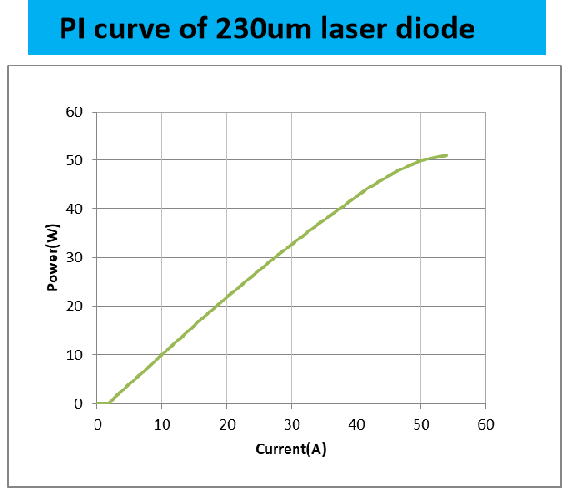
Figure Typical broad-stripe laser lateral brightness is limited by the far field. Temperature non-uniformity, rather than average temperature, causes far-field blooming. We developed a novel high-brightness laser structure using optimized non-uniform contact metal layers to alter the thermal conductivity profile. As shown in Figure
12, in the optimized structure, waveguide temperature non-uniformity is reduced by more than 30%. 12 Brightness Enhancement 。

Figure Currently, the market demands high brightness, high power, high efficiency, low volume, and low weight fiber-coupled modules. To achieve this goal, there are two approaches: one is to improve at the chip level, and the other is to enhance output brightness through optical beam combining technology. Obviously, brightness and power cannot be simultaneously improved by free-space beam combining, as can be seen from simulations,
where 12 beams almost fill the NA, but the tails along the fast axis penetrate into the cladding, which is very dangerous because beams exceeding the NA or entering the cladding will burn the coating, as shown in Figure 13. Adding more beams exceeds fiber limits, so we need to find a new method to further improve brightness, power, and efficiency. For optical beam combining technology, dense wavelength beam combining is a better choice. 13 Fiber-Coupled Pump Optimization
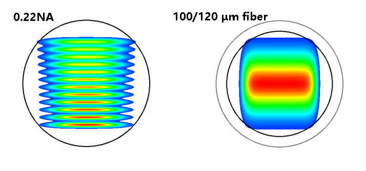
Figure But DWBC alone is not enough. The traditional light source used in DWBC is diode lasers, which suffer from the smile effect that reduces brightness. Moreover, under the same current density conditions, the polarization ratio is lower compared to single-bar sources. When abnormal polarization states exist in the cavity, this causes additional power loss. We use single bars to avoid the smile effect and thermal crosstalk. The assembly flowchart of our high-power, high-brightness, high-efficiency fiber-coupled modules can be divided into five steps (as shown in Figure 14): (1) mounting bare chips on aluminum nitride substrates, (2) spatial stacking of chips on copper submodules, (3) dense spectral beam combining of all chips, (4) further power enhancement using a polarization beam combiner while maintaining the same beam quality, (5) coupling the combined beam into the fiber.
14 High-Power, High-Brightness, High-Efficiency Fiber-Coupled Module Assembly Process Through complex epitaxial design and process control,
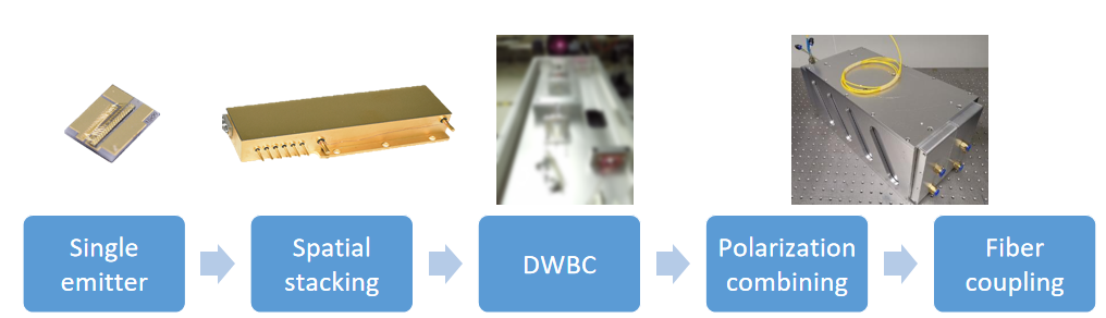
Figure μ
通过复杂的外延设计和工艺控制,120μ The single-bar chip with m luminous area width can output 13W at 14A, with a PCE of 63.1%, while the divergence angles of both axes are well controlled. Divergence angle is a very important parameter as it determines the fiber coupling efficiency in DWBC based on single-bar chips. This differs from DWBC based on laser diode bars. In DWBC based on single-bar chips, the near field of the chip affects the final fiber output divergence angle, while the far field of the chip determines the coupling efficiency. Therefore, the divergence angle of the fiber coupling module will not increase with increasing current. The NA improves because the chip's near field contracts at high current.
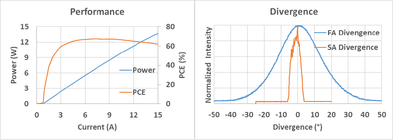
Figure 15 High-performance 120 μm Laser Chip
We developed a “Artificial Laser Diode Bar” with 12 single-bar chips featuring low smile and high polarization ratio. The fast and slow axes are collimated in the module, but residual divergence remains too large. This is why both axes need to be re-collimated. The distance between each chip in the module is large to avoid thermal crosstalk. Therefore, passive cooling can provide good heat dissipation for the module, simplifying the heat dissipation structure. The polarization ratio of this module reaches up to 95.6% at high current, meaning that using polarization-related optical components for beam combining can still maintain very high efficiency.
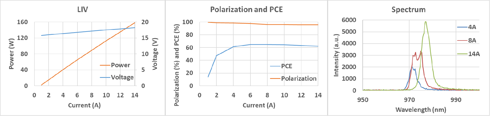
Figure 16 High-performance M12 Module with 120μm Chip
All submodules based on single-bar chips output beams that are ultimately focused into a 100μm fiber. To improve the beam quality of the fast axis, all M12 modules are rotated 90 degrees, as shown in Figure 17. The three submodules on the left and the three on the right are spectrally combined by a transmission grating, then a polarization beam splitter cube combines the two 300W combined outputs through polarization beam combining, doubling the brightness. An aperture diaphragm is placed before the focusing lens to ensure 100% of the light is contained within 0.17 NA, guaranteeing the final fiber output divergence angle.
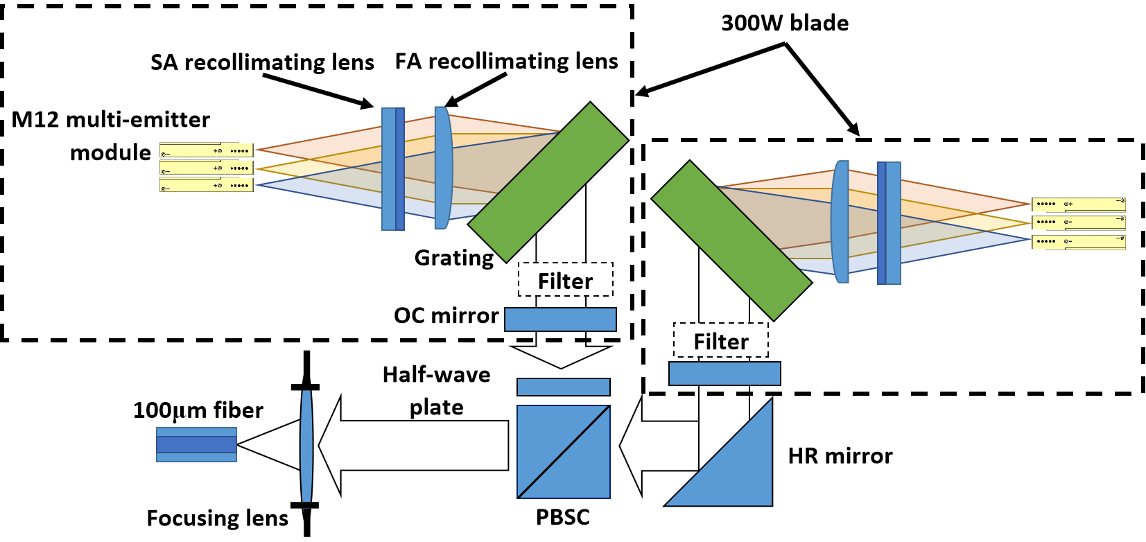
Figure 17 Rotating the M12 module 90° to apply DWBC in the fast axis direction
All results align with our design goals except for the spectral width ( FWHM), which is 0.2nm larger than expected because the wavelengths of the two 300W engines do not completely overlap. At 400W output, the PCE peak is 51.3%. A record ultra-high output power of 687W was achieved at an operating current of 14A. These results also demonstrate the potential of fiber coupling modules based on dense spectral beam combining technology with single-bar chips.
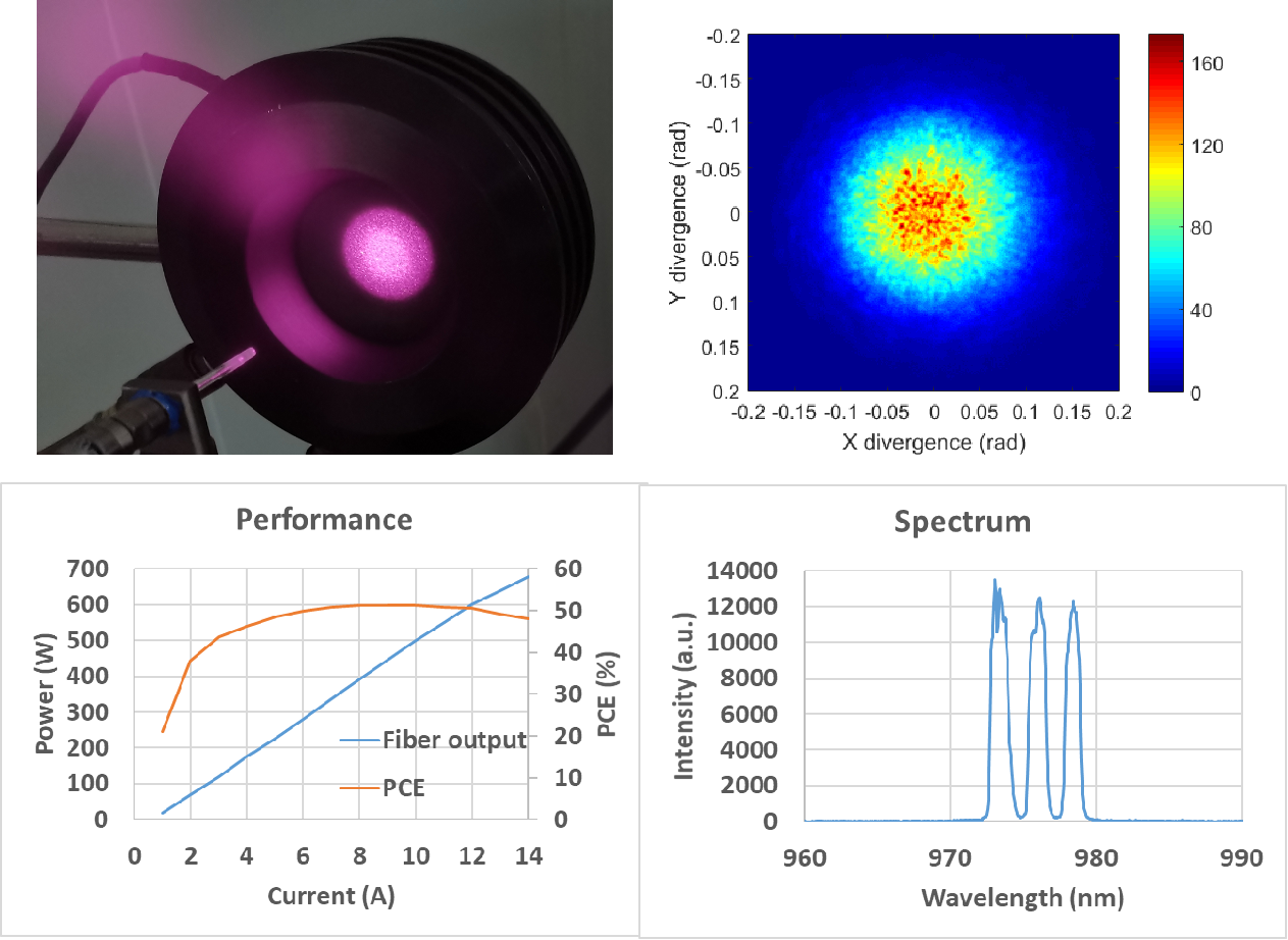
Figure 18 600 W/100 μm Fiber Coupling Module
2.5 1 μm Laser Photovoltaic Chip and Module
Figure Figure 19 shows the structural design and material characterization of the GaAs/InGaAs lattice-mismatched buffer layer. We proposed a structural design combining compositional stepping with compositional overshoot and compositional rollback, achieving simultaneous control of buffer layer lattice relaxation and surface roughness, effectively reducing threading dislocation density (TDD < 1×10 6 cm -2 ).

Figure 19 Characterization of Surface Roughness, Lattice Relaxation, and Threading Dislocations of GaAs/InGaAs Lattice-Mismatched Buffer Layer
On this lattice-mismatched buffer layer, a 1 μm laser photovoltaic absorption region was grown, and under 1 μ μm laser irradiation, its photoelectric conversion efficiency reached 44.1%. Stable output without attenuation lasted for 550 hours under 4W laser irradiation.
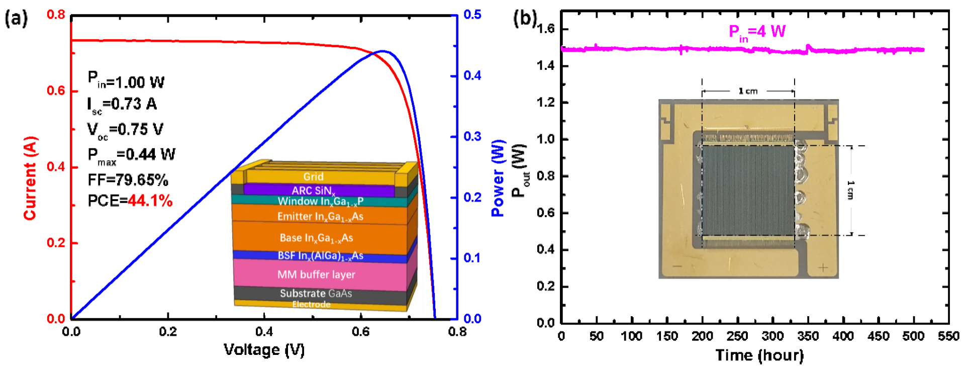
Figure 20 (a) I-V curve of InGaAs lattice-mismatched laser photovoltaic cell under 1064nm laser irradiation. (b) Reliability test [6].
3.0 Summary
This paper reports the latest achievements of our research team in all-semiconductor laser wireless power transfer chips and systems, including 808 nm and 1 μ μm emitting laser chips and modules, single/multi-junction laser photovoltaic chips and modules at the receiving end, and the latest progress in laser wireless power transfer systems.
4.0 Acknowledgments
Thanks to Suzhou Changguang Huaxin Optoelectronics Co., Ltd. and Sichuan University for their support of this work.
References
[1]C. Algora, I. García, M. Delgado, R. Peña, C. Vázquez, M. Hinojosa, and I. Rey-Stolle, "Beaming power: Photovoltaic laser power converters for power-by-light," Joule (2021).
[2]K. Jin and W. Zhou, "Wireless Laser Power Transmission: A Review of Recent Progress," IEEE Transactions on Power Electronics 34, 3842-3859 (2019).
[3]S. Fafard and D. P. Masson, "Perspective on photovoltaic optical power converters," Journal of Applied Physics 130(2021).
[4]M. C. York and S. Fafard, "High efficiency phototransducers based on a novel vertical epitaxial heterostructure architecture (VEHSA) with thin p/n junctions," Journal of Physics D: Applied Physics 50, 173003 (2017).
[5]Y. Gou, H. Wang, J. Wang, R. Niu, X. Chen, B. Wang, Y. Xiao, Z. Zhang, W. Liu, and H. Yang, "High-performance laser power converts for direct-energy applications," Optics Express 30, 31509-31517 (2022).
[6]Y. Gou, H. Wang, J. Wang, Y. Zhang, R. Niu, X. Chen, B. Wang, Y. Xiao, Z. Zhang, and W. Liu, "1064 nm InGaAs metamorphic laser power converts with over 44% efficiency," Optics Express 30, 42178-42185 (2022).
[7]L. Juan, Y. Hao, Y. Tiancheng, G. Yudan, Y. Huomu, and W. Jun, "Design of high efficiency diode laser module for wireless power transmission," Infrared and Laser Engineering 50, 20210147-20210141-20210147-20210148 (2021).
Recommended Reading

Address: No.56,Lijiang Road,SND,Suzhou,Jiangsu Province,P.R.China
Mailbox:sales@everbrightphotonics.com
Website:www.everbrightphotonics.com
Phone:+86 0512-66896988
Fax:+86 0512-66806323
Message Board